Abstract
Graphitic carbon nitride (g-CN), as a potential photoelectrode for photoelectrochemical water splitting, has garnered significant research attention owing to its favorable attributes, including a suitable bandgap, abundant elemental composition, excellent thermal stability, and non-toxicity. However, the limited efficiency of visible light absorption and poor electrical conductivity of pure g-CN result in low photocurrent density and photocatalytic activity, falling short of meeting the requirements for commercial applications. In contrast, graphitic carbon materials possess high conductivity and stability, appearing to be an excellent candidate for enhancing the photocatalytic performance of g-CN while maintaining its stability. Recently, nitrogen vacancies, surface junction, carbon crystallite introduction, and carbon atom doping methods have been employed to prepare carbon-modified g-CN. The introduced π-electron conjugated system by sp2-hybridized carbon atoms indeed extends the visible light absorption and photocurrent of g-CN, resulting in improved photocatalytic performance. In this review, we highlight recent advancements in the development of carbon-modified g-CN and offer insights into the future prospects of g-CN-based films.
1 Introduction
Solar energy, as an abundant and environmentally friendly resource, presents a promising solution to meet the high consumption of finite fossil fuels and the growing energy demands of human society [1,2,3]. Photocatalytic process has been proven to be an efficient approach to harness and convert intermittent sunlight into transportable chemical fuels, reducing greenhouse gas emissions in the process [4, 5]. As an illustration, the photoelectrochemical (PEC) water-splitting reaction, which mirrors natural photosynthesis, emerges as a viable artificial strategy for generating hydrogen gas, representing a significant move towards cleaner energy sources, thereby mitigating global energy shortages and environmental issues. In 1972, Fujishima and Honda achieved a pioneering breakthrough by successfully employing PEC cells to generate hydrogen and oxygen gases separately when exposing the photoelectrode to light irradiation [6], thus preventing the dangerous mixture of oxygen and hydrogen into explosion gas. Consequently, PEC devices have been recognized as a straightforward method for attaining the solar-to-chemical energy objective, relying solely on semiconductors to integrate electrocatalytic and light-absorbing functionalities. In the realm of water-splitting PEC cells, semiconductor materials, such as TiO2 [7,8,9,10,11], BiVO4 [12,13,14], ZnO [15, 16], among others [17], are crucial, serving as primary components for capturing and converting solar energy into chemical fuels. Specifically, graphitic carbon nitride (g-CN or g-C3N4), due to its affordability, non-toxicity nature, and high stability, has garnered considerable interest in this field [18,19,20,21,22,23,24,25,26]. Additionally, g-CN can be easily synthesized from cost-effective nitrogen-rich and oxygen-free compounds containing C–N core structures, such as thiourea, dicyandiamide, and melamine [4]. Therefore, since its initial use in 2009 [26], significant dedication of effort has been focused on exploring the potential of g-CN in PEC devices.
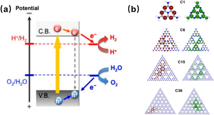
In the PEC system, the absorption of sunlight by the g-CN materials possessing an appropriate bandgap (2.7 eV) is adequately substantial to overcome the endothermic energy of the water-splitting reaction [4]. The electrons are excited from the valence band (VB) or the highest occupied molecular orbital (HOMO) to the conduction band (CB) or the lowest unoccupied molecular orbital (LUMO) of the photoelectrode to reduce the H+ producing H2 gas (2H+ 2e− → H2) in the water-splitting process (Fig. 1a) [1, 27]. Meanwhile, the remaining hole in the VB or HOMO facilitates the oxidation reaction, releasing O2 gas (2H2O → 4H+ + O2 + 4e−). Therefore, the water-splitting process can be delineated into three fundamental steps: (1) light absorption, (2) transfer and separation of photoinduced electron and hole charge carriers, and (3) redox reactions. However, a noteworthy concern is the large bandgap of g-CN, limiting its utilization of visible light. Besides, the high recombination rate of partially separated photoinduced charge carriers also reduces the photocatalytic activity of g-CN for water splitting (Fig. 1b) [28]. To address these issues, surface junctions, which can separate photoinduced electrons and holes onto distinct surfaces, have been employed. For example, gold (Au) clusters were combined with g-CN (Au/g-CN) by electrophoretic deposition and ultrasonication methods [29]. The plasmonic effects induced by Au extend the efficiency of visible-light absorption and enhance photocurrent density. Semiconductor oxide nanoparticles, such as Cu2O [30], TiO2 [31], BiVO4 [32], and Fe2O3 [33], have been utilized to establish surface junction structures for high photocatalytic activity. Moreover, Xiong et al. used the multiple-step thermal vapor condensation (MSTVC) approach with thiourea (CH4N2S) as precursors, reacting with the fluorine-doped tin dioxide (FTO) layer to synthesize the SnS2/g-CN composite [34]. As S atoms possess a greater number of valence electrons compared to N, this method enables the excitation of more electrons, ultimately enhancing photocurrent density of 844.6 µA cm−2 at 1.23 V vs. RHE under AM 1.5G illumination. Hence, surface junction has been demonstrated as an effective strategy in enhancing the photocatalytic performance of g-CN films.
a Schematic illustration of water splitting over semiconductor photocatalyst. Reprinted with permission from Ref. [1]. Copyright 2011 Elsevier. b Frontier orbitals display of the g-CN in the ground state of various dimensions. Dark brown (dark green) isosurface color indicates HOMO (LUMO) wave functions. Reprinted with permission from Ref. [27]. Copyright 2018 Wiley
Doping is another widely used approach for modifying the bandgap and augmenting the charge transfer process in g-CN materials. Typically, metal or nonmetal dopants replace nitrogen or carbon atoms within the g-CN structure, broadening the light absorption range and effectively curbing charge recombination. Ag, as the first metal dopant, doped g-CN was successfully synthesized by Liu et al., with current density increased to 6.4 μA/cm2 [35]. A higher current density of 69.8 μA/cm2 was achieved using a liquid-based growth method where Ni atoms were strategically positioned within the vacancies of g-CN [36]. For metal-free doping, B was incorporated into g-CN by replacing carbon atoms through a thermal vapor condensation (TVC) process, employing a mixture of melamine and boron as precursors [21, 37]. This approach resulted in an almost fourfold increase in photocurrent density compared to pristine g-CN films. Similarly, O-doped g-CN also exhibited improved photocatalytic performance [25], with the introduction of O heteroatoms creating new bandgap states that enable the absorption of visible light across the spectrum. Apart from atom substitution, nonmetal atoms can also bind to the g-CN film through van der Waals (vdW) forces, electrostatic interactions, hydrogen bonding, or π–π stacking, resulting in a charge transfer complex in the stacking structure. This method was known as the charge transfer doping method [38]. For example, I3− and I5− clusters, as well as Ag atoms, were implanted into the g-CN film by noncovalent attachment [39]. The p orbitals of polyiodides facilitated electron tunneling, thus enhancing charge carrier transfer and separation. Additionally, Tian et al. conducted an in-depth investigation of the noncovalently iodinated g-CN film [40]. The I− species introduced additional bandgap states and subsequently reduced the bandgap, leading to enhanced light absorption efficiency and improved charge carrier separation. Therefore, both conventional doping and charge transfer doping approaches have the potential to enhance the photocatalytic performance of g-CN films.
Due to its good electrical conductivity owing to C–C π bonds, cost-effectiveness, widespread availability, and relatively high chemical stability, carbon (C) is regarded as one of the premier materials employed for the modification of carbon-based catalysts [41]. Additionally, nitrogen vacancies (NVs) can lead to the C-rich g-CN, and it has been demonstrated that C–C π bonds have the capacity to reduce the bandgap of g-CN, thereby extending its light absorption capabilities into the visible spectrum [23, 24]. These bonds also play a vital role in enhancing conductivity, resulting in improved transfer of photoinduced charge carriers. Therefore, to construct C-modified g-CN (C/g-CN) structures, besides the C–C π bonds introduced by NVs, C has also been extensively applied in both surface junction and doping methods, leading to the introduction of various C structures, including C surface [42,43,44,45,46,47,48,49,50], C crystalline [51,52,53,54,55], and C atoms [56,57,58,59,60], into g-CN films. These kinds of C/g-CN photocatalysts are summarized in Table 1. In this review, we provide an overview of the recent developments in C/g-CN films.
able 1 Summary of different kinds of C-modified g-CN photocatalysts
| Photocatalyst | Synthesis method | Structure | Photocurrent (μA cm−2) |
|---|---|---|---|
| NV/g-CN | Annealing [24], temperature-controlling route method [61] | NVs in the plane | About 75 (0.1-m Na2SO4, 0.1-m Na2SO3, and 0.01-m Na2S under a NEWBET AM 1.5-G solar simulator at 1.23 V vs. RHE) [24] |
| Graphene/g-CN | Impregnation-chemical reduction and calcine [42] | Surface junction | About 25 (1-M Na2 SO4 under visible-light irradiation at 0.5 V vs Ag/AgCl) [42] |
| CNT/g-CN | Combined solvothermal and ultrasonic methods [44], steaming treatment [45] | Combined through hydrogen bonds [44] or covalent bonds [45] | About 1 (under a 300-W Xe lamp) [44] |
| CQD/g-CN | Thermal polymerization and ultrasonic treatment [46] | Surface junction | About 0.4 (0.50-m Na2SO4 under Xe lamp illumination at 0.8 V vs Ag/AgCl) [46] |
| Cring/g-CN | Multiple-step thermal treatment [52], modified gas-shocking strategy [53] | π-conjugated bonds in the plane | Over 1 (0.3-m Na2SO4 under 300-W Xe lamp) [53] |
| Catom/g-CN | Thermal vapor condensation method [23], one-step thermal condensation [58], impregnation-assisted calcination [60] | C dopants in the plan | About 30 (0.5-m Na2SO4 under a Xenon lamp at 1.0 V versus RHE) [60] |
2 C-modified g-CN films
2.1 Nitrogen vacancies decorated g-CN (NV/g-CN)
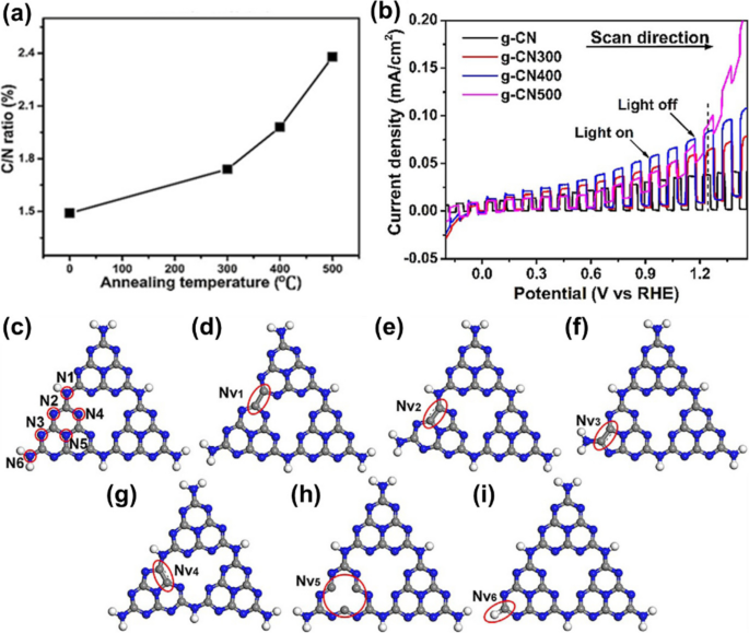
To remove the N atoms and form NVs, Bian et al. employed an annealing method [24]. Following the production of g-CN films at 600 °C using the TVC method (Table 1), the samples underwent annealing at temperatures of 300, 400, and 500 °C (Fig. 2a), named g-CN300, g-CN400, and g-CN500, respectively, under a continuous flow of nitrogen (N2) flow. With higher temperatures, a greater number of N atoms became detached from the g-CN film. Consequently, the photocurrent density was highly improved due to the newly formed C-C π bonds, as shown in Fig. 2b. Additionally, the temperature-controlling route method can also be used to introduce NVs in the g-CN films, extending their visible light absorbance between 450 and 600 nm [61]. Theoretically, the Nv/g-CN was studied by the SCC-DFTB method. As illustrated in Fig. 2c, d, e, f, g, h, and i, there are six possible sites for Nv [20, 62]. At NV4, the structure exhibited the lowest energy, indicating its highest degree of stability and the most favorable geometry, confirming the formation of the newly formed C–C π bonds by the C atoms adjacent to NV. Owing to the newly formed C–C π bonds, the valence and conduction bands of NV/g-CN both move to lower energies. Additionally, compared to the bandgap (2.82 eV) of pristine g-CN, the bandgap of NV/g-CN decreases to 2.52 eV, indicating higher absorption efficiency under visible light [62]. Because of the symmetry disruption caused by NV, both the newly formed C-–C π bonds and existing C–N π bonds contribute to the enhancement of photoinduced charge transfers, resulting in a higher experimental photocurrent density. Therefore, the introduction of NVs can significantly enhance the performance of g-CN films. However, further improvements are essential for potential commercialization.
a C/N ratio of the pristine and the annealed g-CN films. An annealing temperature of “0 °C” denotes the pristine g-CN film. b Linear sweep voltammetry (LSV) curve of the pristine and the annealed g-CN films under chopped light. The dotted line marks the photocurrent density at 1.23 V vs. RHE. c A schematic model of the g-CN sheet constructed by tri-s-triazine. The gray, blue, and white spheres stand for C, N, and H atoms, respectively. Six kinds of N atoms are highlighted by red cycles, which are designated as N1–N6. d, e, f, g, h, i Calculated structures of the g-CN sheet in c with different N atoms absent. d NV1, e NV2, f NV3, g NV4, h NV5, and i NV6. Reprinted with permission from Ref. [24]. Copyright 2017 Wiley
2.2 C-surface/g-CN composites
2.2.1 Graphene-decorated g-CN (graphene/g-CN)
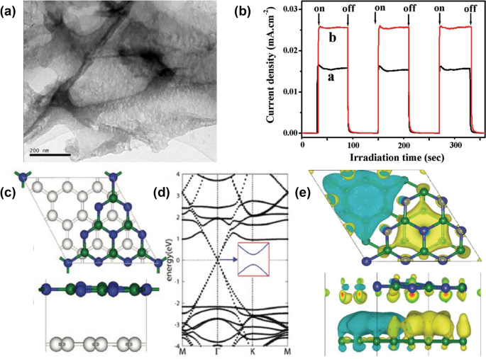
Graphene, a two-dimensional layer composed of carbon atoms possessing a honeycomb structure, has garnered widespread attention owing to its outstanding mechanical, thermal, optical, and electrical properties [63,64,65]. In particular, due to its sp2 hybrid carbon atoms, graphene exhibits excellent mobility of charge carriers (200,000 cm2 V−1 s−1) and an extremely large specific surface area (∼2600 m2/g) [42]. As a result, it has gained wide utilization in enhancing the conductivity of other catalysts through the construction of surface junction structures. In 2011, the graphene/g-CN (Fig. 3a) photocatalyst for hydrogen production was synthesized through thermal treatment, creating a layered structure from melamine and graphene oxide precursors [42]. The graphene content determined to be ∼1.0 wt %, resulting in a broad-spectrum background absorption in the visible-light region, as well as serving as conductive channels to improve the transfer and separation of photointroduced charger carriers. As depicted in Fig. 3b, the significant increase in photocurrent of graphene/g-CN was indicative of reduced recombination and more efficient separation of charge carriers. The corresponding H2-production rate reached 451 μmol h−1 g−1, surpassing that of pure g-CN by a remarkable factor of over 3.07 times. Meanwhile, a theoretical study constructed a hybrid graphene/g-CN structure (Fig. 3c) revealing that the electronic properties of the energy band closely resembled those of pure graphene rather than g-CN (Fig. 3d) [43]. Charge density differences within the graphene/g-CN structure highlighted the prevailing existence of triangular-shaped regions of electrons and holes, primarily localized in the graphene layer (Fig. 3e). This observation underscores the substantial role of graphene in facilitating conductive pathways. Similar to the experimental findings, the calculated absorption spectrum of this hybrid complex significantly extended, covering a range from UV light to visible spectrum.
a TEM images of graphene/g-CN. b Transient photocurrent responses of the pure g-CN (marked as line a) and graphene/g-CN (marked as line b) samples in 1-M Na2SO4 aqueous solution under visible-light irradiation at 0.5 V vs Ag/AgCl. Reprinted with permission from Ref. [42]. Copyright 2011 American Chemical Society. c Optimized graphene/g-CN interface in a top view and a side view. d Calculated band structure by the HSE06 functional for graphene/g-CN. e Charge transfer at the graphene/g-CN interface: top and side view of the three-dimensional charge density difference plots. Green and blue balls represent C and N atoms, respectively. Yellow and light blue isosurfaces represent, respectively, charge accumulation and depletion in the space with respect to isolated graphene and g-CN. Note the triangular-shaped electron-hole puddle. The isovalue chosen to plot the isosurfaces is 0.002 e/Å3. Reprinted with permission from Ref. [43]. Copyright 2012 American Chemical Society
2.2.2 Carbon nanotubes decorated g-CN (CNT/g-CN)
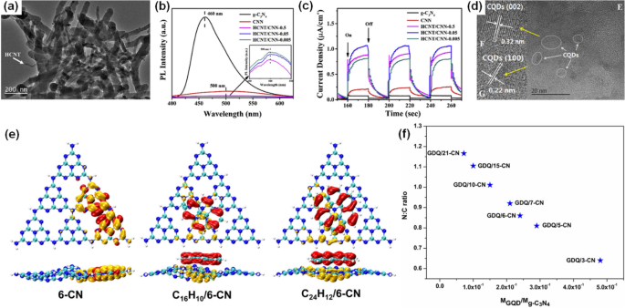
Similar to graphene, carbon nanotubes (CNT) are formed from sp2 hybridized carbon atoms, resulting in high electrical conductivity, making them excellent materials for enhancing charge transfer in g-CN. As shown in Fig. 4a, the carbon nitride nanobelt (CNN) was combined with the hydroxyl-containing CNT (HCNT) through hydrogen bonds formed between the hydroxy groups on HCNT and the amino groups present on the surface of CNN [44]. The PL spectra showed that the signals decreased more significantly with an increase in HCNT content within the HCNT/CNN composites (Fig. 4b), suggesting reduced rates of recombination of photoinduced electron-hole pairs. Additionally, this modification enabled the composites to convert visible light into photocurrent efficiently and facilitated the easier excitation of charge carriers. As a result, the photocurrents of HCNT/CNN composites, with varying HCNT content of 0.5, 0.05, and 0.005 by weight, were notably higher than those of pure g-CN and CNN (Fig. 4c). Notably, the current intensity of HCNT/CNN-0.05 was approximately five times higher than that of CNN, underscoring that the incorporation of HCNT enhanced the efficiency of separating photoinduced charge carriers. In addition to weak interactions, Zhao et al. combined amine-rich g-CN, synthesized using the dicyandiamide-blowing method, with CNTs by covalent bonds via an amidation reaction [45]. XPS spectra revealed an increase in C–C groups and a decrease in C–NH2 groups, confirming the covalent binding of CNTs to g-CN, which also promoted the efficient transfer of photoexcited charge carriers and minimized the recombination of them.
a Typical TEM image of HCNT/CNN-0.05 containing 0.5 wt% of HCNT. b PL spectra. c Photocurrent under visible light. Reprinted with permission from Ref. [44]. Copyright 2019 Elsevier. d HRTEM (E-G) images of CQD/g-CN. Reprinted with permission from Ref. [46]. Copyright 2016 Elsevier. e Electron-hole (orange-red) distribution in S1 geometries of 6-CN, C16H10/6-CN, and C24H12/6-CN. f Nitrogen-to-carbon (N:C) ratio as a function of the molecular mass ratio of GQD to g-C3N4 (MGQD/Mg-C3N4) in GQD/g-C3N4 system. Control over the N:C ratio regulated the electron-hole separation in the modified g-C3N4 structure. Reprinted with permission from Ref. [50]. Copyright 2019 Elsevier
2.2.3 Carbon quantum dots decorated g-CN (CQD/g-CN)
Carbon quantum dots (CQDs), typically smaller than 10 nm, are synthesized by the “bottom-up” method via the thermal treatment of molecular precursors [41]. As a new novel class of quasi-spherical carbonaceous nanocarbons, these materials are composed of amorphous to nanocrystalline cores in which graphitic carbon (sp2 carbon) or graphene is integrated with diamond-like sp3 hybridized carbon insertion. Like graphene and CNT, CQDs possess good electrical conductivity, making them suitable candidates for enhancing the photocatalytic activity of g-CN [46,47,48,49]. Under ultrasonic treatment, g-CN can be easily combined with different contents of CQDs in absolute ethanol (Fig. 4d) [46]. The CQD modification lowers the bandgap of g-CN from 2.83 to 2.80 eV, leading to a redshift in the absorption edge, and the reduction in PL emission intensity after the introduction of CQDs indicated less recombination of photoinduced charge carriers. Under UV-vis irradiation (100 mW cm−2) at 0.8 V vs Ag/AgCl, CQD/g-CN achieved a photocurrent density twice that of pure g-CN. Meanwhile, the improved photocatalytic activity of CQD/g-CN was proved by a theoretical study using density functional theory (DFT) and time-dependent DFT (TD-DFT) computations [50]. As illustrated in Fig. 4e, CQD/g-CN was formed through the interaction of g-CN bonded with CQDs via the π-π stacking, where the C16H10 and C24H12 were employed to simulate the CQD. In pure g-CN composed of six heptazines (6-CN), both the HOMO and LUMO are located in the same area. Because, after light absorption, the electrons are mainly emitted from HOMO to LUMO. Hence, the photoinduced electron-hole pairs are not efficiently separated. On the contrary, for C16H10/6-CN and C24H12/6-CN, the HOMO is primarily located in the CQD, whereas the LUMO is predominantly in the g-CN. Consequently, upon light excitation, the electrons are transferred to the g-CN, resulting in the photoinduced charge carriers being individually situated in the CQD and g-CN, respectively. Moreover, the sizes of g-CN and CQD affect the separation of photoinduced charge carriers of CQD/g-CN. Fig. 4f showed the nitrogen-to-carbon ratio as a function of the GQD to g-CN molecular-mass ratio, a large N:C ratio indicates the primary contribution from the g-CN nanosheet with a lower MGQD/Mg-C3N4 ratio, and the lowest N:C ratio signifies the dominant role of GQDs. In particular, when the N:C ratio falls within the range of 0.8–1.0, with a molecular mass ratio ranging from 1.5 × 10⁻¹ to 3.0 × 10⁻¹, it leads to improved separation of photoinduced charge carriers in CQD/g-CN. This provided a theoretical insight into GDQ/g-CN and the ideals for its experimental synthesis.
Therefore, sp2 hybridized carbon structures in C-surface/g-CN composites can enhance the photocatalytic activity. Owing to the surface junctions in C-surface/g-CN composites and upon light absorption, the photoinduced electron and hole may be separated and located at different layers. Thus, the electron-hole pairs recombination can be prevented, indicating prolonged fluorescent lifetime of C-surface/g-CN compared to that of pristine g-CN. The better separation of photoinduced electron and hole leads to longer lifetimes of charge carriers and a higher probability of participation in photocatalytic reactions, improving the photocatalytic performance.
2.3 Carbon crystalline (Cring)-conjugated g-CN (Cring/g-CN) composites
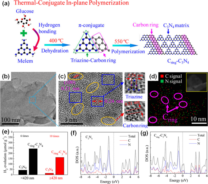
In 2017, carbon crystallite was first incorporated into the g-CN plane through π-conjugated bonds (Cring/g-CN) [52]. To synthesize Cring/g-CN, melamine powders were mixed with glucose, followed by the multiple-step thermal treatment (Fig. 5a). The glucose molecules bonded to melamine by in-plane sp2-hybridized C–N bonds, forming carbon crystallite, named C ring (Cring) (Fig. 5b, c, d). The C–C bonds of Cring can directly transport the photoinduced charge carriers to the catalytic active sites, thus improving their separation efficiency. The transient open-circuit voltage decay (OCVD) measurements proved that the open-circuit voltage of Cring/g-CN exhibited a prolonged decay after light was turned off, implying a longer lifetime for photoinduced charge carriers. Cring/g-CN, due to the extended light absorption in the 500–800 nm range to pure g-CN, demonstrated higher visible light utilization. Therefore, its H2 production rate reached up to 150 μmol g−1 h−1 under irradiation of visible light (≥ 420 nm), 10 times higher than pure g-CN. Recently, citric acid [53], polyvinyl butyral [54], and hexaketocyclohexane octahydrate [55], containing sp2 hybridized carbon cores, were also employed to serve as the source of carbon crystallite. Same as glucose, the N–C bonds were formed to combine the carbon crystallite with g-CN under the thermal polymerization process. DFT calculations provided a deep insight into the correlation between the in-plane heterostructure and photocatalytic activity [52]. Based on the densities of states (DOS) (Fig. 5f and g), in contrast to pure g-CN, Cring/g-CN possesses a new intermediate energy level located at approximately 0.5 eV with the Fermi level intersecting this band state, compared to pure g-CN. The clearly reduced bandgap in Cring/g-CN corresponded well with the expanded absorption of visible light. Moreover, the substantial presence of mobile electrons near the Fermi level considerably boosted the water adsorption energy in Cring/g-CN to 1.10 eV, compared to the 0.90 eV observed in pure g-CN. The enhanced adsorption resulted in higher photocatalytic activity for water splitting. Hence, the synergistic effects between carbon crystalline and g-CN have been proved by both experimental and theoretical studies. However, the synthesis method is kind of cumbersome, and the impacts of varying carbon crystalline contents still require further investigation. For Cring/g-CN, a more comprehensive understanding of the separation as well as distribution of photoinduced charge carriers in excited states in theory is still needed.
a Synthetic route for the in-plane heterostructure of (Cring)-C3N4. b TEM image and c HRTEM image for the sample. The elliptic area represents carbon ring, and the rectangular area is C3N4 matrix. d EDS mapping of (Cring)-C3N4. The inset of TEM image shows the corresponding region for mapping. e H2 evolution under UV (< 420 nm) and visible light (≥ 420 nm) per hour. f and g Calculated DOSs for pristine g-C3N4 and (Cring)-C3N4. Reprinted with permission from Ref. [52]. Copyright 2017, American Chemical Society
2.4 Carbon atoms doped g-CN via substitution of N atoms
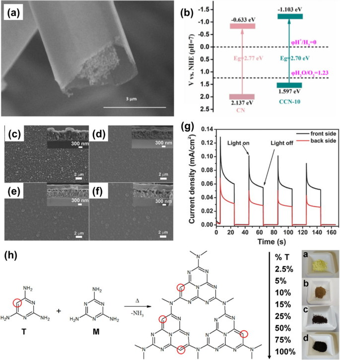
The C atoms doped into g-CN via substitution of N atoms introduce C–C bonds and a π-electron conjugated system, enhancing the electric conductivity and the efficiency of photoinduced charge separation. Glucosamine hydrochloride was employed as the source of C dopants, ensuring its direct incorporation via copolymerization with melamine. As shown in Figure 6a, C atom doped g-CN (Catom/g-CN) was synthesized using 2-g melamine and 10-g glucosamine hydrochloride, named CCN-10 [56]. The introduction of plentiful π-electrons results in a slight reduction of the bandgap to 2.70 eV for CCN-10 (Fig. 6b), compared to the 2.77-eV bandgap of pure g-CN, and notably improves the photocurrent, exceeding twice that of pure g-CN. Remarkably, H2 evolution rate of 3888.9 μmol h−1 g−1 was obtained for CCN-10, four times higher than that of pure g-CN. Recently, Shi et al. introduced a one-step synthesis method using urea and n-octanol as precursors to prepare Catom/g-CN [57]. Similar to Catom/g-CN synthesized with glucosamine hydrochloride, the bandgap was also lowered to 2.71 eV, implying the C atom doping effectively improved the visible-light absorption. To produce the C-rich g-CN (Fig. 6c, d, e, f), Bian et al. used 2,6-diaminopyridine (26D) and melamine through the TVC method to modify the g-CN materials [23]. The C-rich g-CN films synthesized by 1, 5, and 10 wt% of 26D were named as CMD1, CMD5, and CMD10, respectively. It was observed that the 26D significantly enhanced the growth of g-CN films by generating gaseous sp2 C groups at high temperatures. Consequently, the resulting films exhibited a fourfold increase of the photocurrent density photocurrent density (Fig. 6g) compared to the pure g-CN film. Triaminopyrimidine and melamine, structurally similar except for the substitution of a single nitrogen atom with a carbon atom (Fig. 6h), were used in different molar ratios to prepare Catom/g-CN, meanwhile controlling the carbon content [58]. Particularly, when triaminopyrimidine content exceeded 50%, the Catom/g-CN obtained is not a typical n-type semiconductor but rather a p-type semiconductor. In addition, as the carbon content increased, the bandgap decreased from 2.78 eV for pure g-CN to 1.73 eV for Catom/g-CN synthesized solely using triaminopyrimidine. This reduction in bandgap contributes to enhanced photocatalytic activity under visible light, leading to a 40% improvement compared to pure g-CN. Theoretically, it was proved that the C dopants could improve the photocatalytic activity of Catom/g-CN [59]. For Catom/g-CN, owing to the lower electronegativity of 2.55 for the C dopant compared to 3.04 for the N atoms, the electrons are excited and transferred to the neighboring N atoms after light absorption. Therefore, the introduced π-electron conjugated system by sp2 hybridized C atom improves the separation of photoinduced electrons and holes. And the vertical excitation energy of pristine g-CN is about 3.09 eV in the first excited state. For Catom/g-CN, the value is reduced to about 1.14 eV, implying the higher absorption efficiency under visible light. Hence, the mechanisms for the higher activity of Catom/g-CN are elucidated.
a SEM images of CCN-10. b Band structure of CN and CCN-10. Reprinted with permission from Ref. [56]. Copyright 2022, Elsevier. Surface and cross-sectional (insets) morphologies of c the g-CN film and d, e, f the modified CN films: d CMD1, e CMD5, and f CMD10. g The transient photocurrent density of CMD5 under 1.23 V versus RHE recorded under front- and back-side illumination. Reprinted with permission from Ref. [23]. Copyright 2016 Wiley. h Postulated thermal condensation of melamine (M) and different % mol of triaminopyrimidine (T) to obtain C-doped carbon nitride. On the right, pictures of some synthesized materials grounded to powder (from top: pristine C3N4, CN25, CN75, and CN100). Reprinted with permission from Ref. [58]. Copyright 2018, Elsevier
3 Conclusion
The g-CN is one of the highly potential photocatalysts for water splitting. However, the low absorption efficiency of visible light as well as poor separation and the high recombination of photoinduced charge carriers constrain its photocatalytic activity and broader applications. Because of the good electrical conductivity, the π-electron conjugated system introduced by C–C bonds can narrow the bandgap of g-CN to enhance the visible light absorption and transport the photoinduced charge carriers to active sites resulting in lower recombination of them. Hence, nitrogen vacancy, surface junction, carbon crystallite introduction, and C atom doping methods were employed to implant C–C bonds into the g-CN complex. In this review, we highlight the recent development of C-modified g-CN materials and present some suggestions for further development.
We suggest that for the surface junction complexes, the bonding between the C materials and g-CN should possess sufficient strength to maintain stability after undergoing multiple cycles of water splitting processes. Additionally, the charge transport suffers tremendous resistance at the interface, leading to energy losses and reduced energy conversion efficiency [51]. Further efforts are required to establish a stronger bond between the carbon surface and g-CN while reducing the resistance for charger transfer between them. For carbon crystallite introduction and C atom doping, it is necessary to simplify the synthesis methods and explore alternative precursors. In particular, one should place emphasis on the development of p-type g-CN materials. In addition to the C doping method, other methods should be developed to synthesize p-type g-CN catalysts. Heterojunction complexes comprising p-type and n-type g-CN, as innovative photocatalysts and photoelectronic devices, may be a critical area for future research.


