Abstract
A new type of copper (Cu)-rhodium (Rh)-alloy, Cu(Rh), films is developed by co-sputtering copper and rhodium onto silicon (Si) substrates under an argon (Ar) atmosphere. The new films are next annealed at 600 and 670 °C, or alternatively at 100 and 450 °C, for 1 h. Longer annealing to the films, for up to 8 days, is also conducted to explore resistivity variation. The resistivity of the new 300-nm-thick film is 2.19 μΩ cm after annealing at 670 °C for 1 h and drifts to 2.26 and 2.14 μΩ after annealing at 400 and 450 °C, respectively, for 200 h. A 2.7-μm-thick Sn layer is then thermally evaporated atop the new film for stable flip-chip solder joints; their metal and Cu-Sn intermetallic compound (IMC) growth processes vs. various annealing periods are tested. After annealing at 670 °C, the new 300-nm-thick film’s adhesive strength reaches 44.2 ± 0.01 MPa, which is 11 ~ 12-fold that of their pure Cu counterpart. Some key test results of the new film are disclosed herein, including its X-ray diffraction (XRD) patterns, transmission electron microscopy (TEM) images, secondary-ion mass spectrometry (SIMS), time-dependent dielectric-breakdown (TDDB) lifetime curves, and adhesive strength. The new film’s antibacterial efficacy arrives at an antibacterial ratio of approximately 100% against Staphylococcus aureus (S. aureus) BCRC 10451 for the 300-nm-thick film and approximately 99.82% for the 8 nm film, far superior to that of a pure Cu film, which is 0 with the same annealing temperature range. The new film, hence, seems to be a remarkable candidate material for various industrial applications, such as ultra-large-scale integrated circuits (ULSIC), micro-electronic circuits, printed circuits, flip-chip technology, medical care concerning antibacteria, and the like.
Graphical Abstract
A new type of copper (Cu)-rhodium (Rh)-alloy, Cu(Rh), films is developed by co-sputtering copper and rhodium onto silicon (Si) substrates under an argon (Ar) atmosphere and then annealing the new films at 600 and 670 °C, or alternatively at 100 and 450 °C, for 1 h. Longer annealing to the films, for up to 8 days, is also conducted to explore resistivity variation. The resistivity of the new 300-nm-thick film is 2.19 mW cm after annealing at 670 °C for 1 h and drifts to 2.26 and 2.14 mW after annealing at 400 and 450 °C, respectively, for 200 h. A 2.7-μm-thick Sn layer is next thermally evaporated atop the new film for stable flip-chip solder joints; their metal and Cu-Sn intermetallic compound (IMC) growth processes vs. various annealing periods are tested. After annealing at 670 °C, the new 300-nm-thick film’s adhesive strength reaches 44.2 ± 0.01 MPa, which is 11~12-fold that of their pure Cu counterpart. Some key test results of the new film are disclosed herein, including its X-ray diffraction (XRD) patterns, transmission electron microscopy (TEM) images, secondary-ion mass spectrometry (SIMS), time-dependent dielectric-breakdown (TDDB) lifetime curves, and adhesive strength. The new film’s antibacterial efficacy arrives at an antibacterial ratio of approximately 100% against Staphylococcus aureus (S. aureus) BCRC 10451 for the 300-nm-thick film and approximately 99.82% for the 8-nm film, far superior to that of a pure Cu film, which is 0 with the same annealing temperature range. The new film, hence, seems to be a remarkable candidate material for various industrial applications, such as ultra-large-scale integrated circuits (ULSIC), micro-electronic circuits, printed circuits, flip-chip technology, medical care concerning antibacteria, and the like.
1 Introduction
When compared with aluminum, copper (Cu) exhibits lower electromigration and lower resistivity. When compared with silver or gold, Cu possesses a superior cost advantage. Cu thus is widely adopted in the metallization processes of ULSICs [1, 2], micro-electronic circuits, printed circuits, and the like, mainly in the semiconductor and photoelectronic industries. However, once a Cu layer is deposited onto a substrate, Cu scattering is prone to creep into the substrate; the scattered Cu often interacts with the silicon dioxide or silicon in the substrate, producing oxides that often detrimentally increase the resistivity [3] of the related electronic components. Thus, a barrier layer is often inserted between a Cu layer and a substrate in conventional printed circuits to avert the Cu scattering.
The barrier layer, however, has a drawback. As the miniaturization trend continues, the printed circuits diminish into nanometer ranges. Under the ranges, the electronic diffraction effect from crystal boundaries deteriorates, increasing the resistivity in the circuits harmfully. It is thus imperative for the semiconductor industry, photoelectronic industry, and the like, to advance a method to prevent copper scattering without the barrier layer. The method is also called barrierless metallization (BM). BM can simplify electronic components’ manufacture and reduce their costs and sizes, to say the least; hence, an optimal BM is highly sought after and to be pursued in the related industries.
BM can be derived into the following application. With the constant miniaturization trend, electronic packaging methods adopting wire bonding between chips have become too bulky and inadequate. The methods are being replaced with flip-chip technology using bumps instead of wires. The technology has been widely used in high-level computer equipment, which requires greater performance, input–output (I/O) density, and cooling. The technology meets the needs of new communication products in several aspects, such as high I/O value and signal transmission quality. The technology has been adopted in portable consumer products, which often have many aggregation and automotive parts needing to withstand harsh temperatures, humidity, and electromagnetic interference. The flip-chip technology is also essential in liquid–crystal-display-driven IC products that are often required to be compact and lightweight. In recent years, the technology and the wafer-level chip-scale packaging (WLCSP) method have been applied to the packaging of many electronic components. Lead-free-solder-bump demand has risen consequently. The bumps are normally deposited by a sputtering or electroplating technique, which partly constitutes under bump metallurgy (UBM). UBM ensures solder wettability, creates a diffusion barrier between a pad and a solder, and provides sufficient adhesion and adequate electrical conductivity [4]. Traditionally, UBM adopts Cu as a wetting layer, for Cu can easily scatter into SiO2 or Si. However, Cu needs to retain thermal stability, which is often challenging at high temperatures, and solderability to form an effective diffusion barrier and wetting layer [5]. To improve the Cu wetting layer, other Cu-alloy films have been studied in the literature [6,7,8,9,10,11].
An optimal BM is thus highly sought after in the aforementioned applications. But how can we achieve it? Answering the question is the key motivation and main goal of the present study. A valid BM process for replacing the mentioned barrier layer ought to be achieved by co-sputtering Cu and an adequate immiscible material with an adequate mixture ratio onto a substrate to render substitute Cu-alloy circuits which can hold thermal stability in high temperatures. Throughout many a study in this field, I find that an adequate BM can be achieved by the aforementioned approach via co-sputtering and proper annealing. The Cu(TiBNx) [12] and Cu(AuTiNx) [13] copper-alloy films published are proven successful BM results. The films exhibit high-temperature endurance, such as thermal stability under high temperatures, owing to the films’ unique microstructure [12, 13]. I and co-workers have also found in a few prior studies that the thermal stability of Cu(ReN) alloy films [14] reaches 730 °C, while that of Cu(RuNx) [15] films 680 °C, and that of Cu(RuHfNx) [16] and Cu(NbCNx) [10] films both 720 °C. In addition, Cu(AgNx) films attain low resistivity, ∼2.2 μΩ cm, after annealing at 600 °C [17].
Since Rh exhibits a high melting point (1966 °C) [18], low electric resistivity, and high corrosion resistance, I have tried to properly mix an adequate amount of it to develop a new type of copper-alloy films in the study. In comparison with Cu(Re) alloy films [19] having thermal stability up to 550 °C and the self-assembled 3-aminopropyltrimethoxysilane diffusion barrier having thermal stability up to 500 °C, the new Cu(Rh) film developed from the present study exhibits thermal stability up to 670 °C, the highest among all the films mentioned above. The new films can be applied to all the mentioned fields and the medical-care [20] field for bacteria killing, too.
Cu can kill bacteria within hours by producing oxygen radicals and destroying cell DNA [21, 22]. The more the copper substance exists in an alloy, the greater the alloy’s bacteria-killing efficacy will be. Once copper oxide (CuO) is formed on a copper surface, the Cu’s antibacterial efficacy will be weakened [21]. Mikolay et al. [21] found that the bacteria count is the least on a copper surface, followed by an aluminum surface and, further, a stainless-steel surface. In 1994, Liu et al. [23] found that copper-silver ionization can reduce the positive rate of legionella inside water supply pipes within medical-care institutes, renewing wider attention to kill bacteria with Cu.
2 Experimental procedure
In the study, we explore and develop a new type of 300-nm- and 8-nm-thick Cu-alloy, Cu(Rh), films containing, as measured with an electron probe microanalyzer (EPMA), 0.1, 0.2, 0.3, 0.5, and 0.7 at.% Rh, which constitutes the (nearly) optimal composition structure for the new films. The thickness and thickness variations of the films are measured by TEM. To understand the effect of film thickness on film performance, the film thickness was measured using TEM. The sputtering speed and time for 300 nm film thickness were 300 ± 2 nm (0.04 nm/s, 2.1 h), and 8 nm film thickness was 8 ± 1 nm (0.04 nm/s, 0.06 h). The new films are formed by co-sputtering (150 W magnetron sputtering) Cu and Rh onto Si substrates under an Ar atmosphere, at 7 × 10⁻³ torr, followed by vacuum isothermal annealing at 400, 450, 600, and 670 °C for 1 h. The crystal structures and microstructures of the films before and after annealing are analyzed with XRD, TEM, and the like. In addition, the film resistivity is measured at room temperature using a four-point probe; leakage current characteristics are determined based on the current–voltage curves of the films deposited on a typical SiO2 (350 nm)/Si metal–oxide–semiconductor (MOS) multilayer. The reliability of the tested films is determined by their TDDB lifetime. The adhesion property of the films is measured by their pull-off strength according to ASTM International standard D4541-02.27.
An Sn layer is thermally evaporated atop a Cu(Rh) film to achieve a stable flip-chip solder joint. The thermal evaporation, driven by 220 Vac, 200 to 230 A, starts when the vacuum reaches ∼3 × 10⁻⁶ Torr and lasts for ∼5 h to produce a 2.7-μm-thick Sn layer.
Antibacterial tests are performed using the method outlined in JIS Z 2801 [24], a Japanese industry standard for evaluating the antimicrobial efficacy of antimicrobial products. The results show that the annealed new films exhibit low resistivity, low leakage current, and strong adhesion to Si substrates. No silicides or oxides are formed during vacuum annealing. Antibacterial studies using Staphylococcus aureus BCRC 10451 are carried out, whereas the antibacterial ratio is calculated by Eq. (1) below:
where:
A designates the total bacteria count on pure Cu films after the initial bacteria are exposed on the films for 24 h;
C represents the total bacteria count on the new Cu(Rh) alloy films after the initial bacteria are exposed on the new alloy films for 24 h.
3 Results and discussion
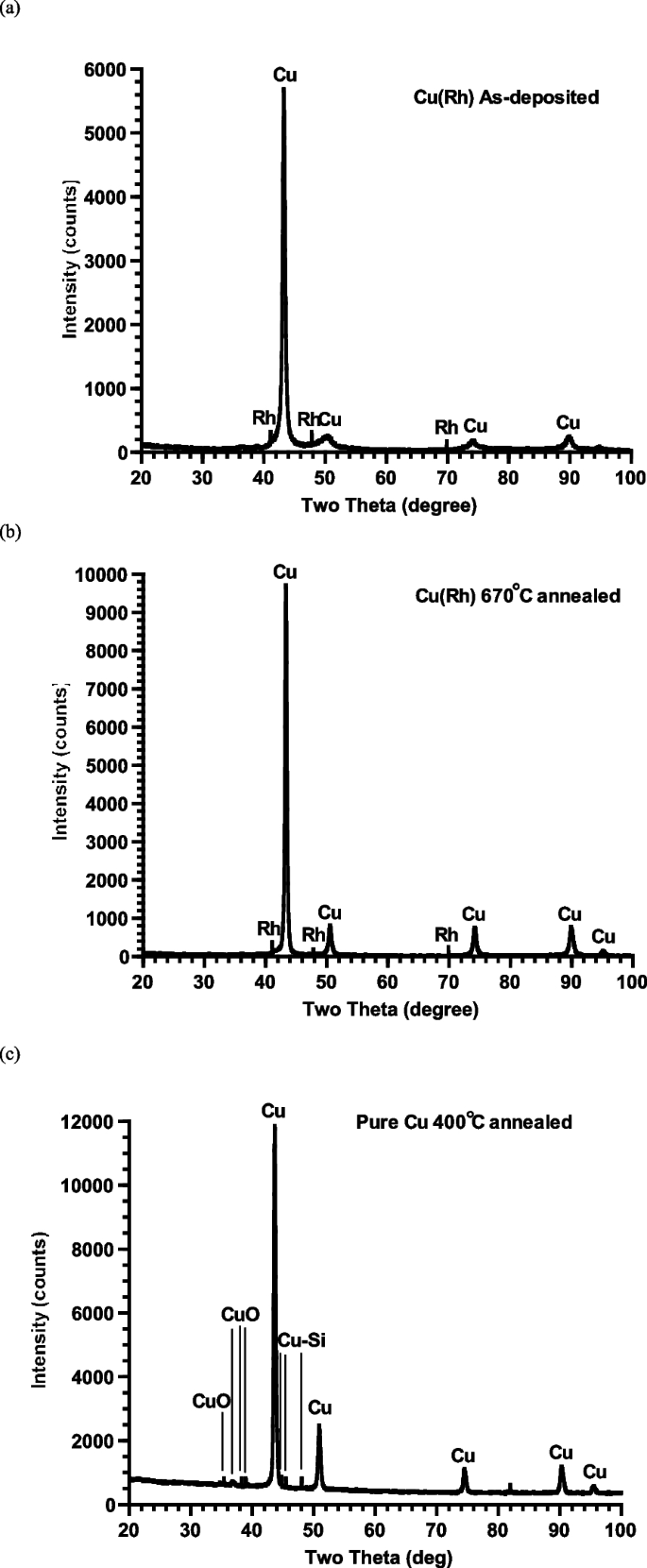
The as-deposited Cu(Rh) films are inspected in Fig. 1(a), where Rh (JCPDS 87–0714) exists and no phase shift of the Cu peak is observed; neither does Cu and Rh-interacted compound incur, viz. no interaction between Cu and Rh is detected. The XRD pattern of the new Cu(Rh) film after annealing at 670 °C is shown in Fig. 1(b), where Rh is dissolved via solid solution process within the film, verifying that the new film holds high-temperature thermal stability. In comparison, CuO and Cu-Si compounds are formed within the pure Cu film (300 nm thick) after annealing at 400 °C as shown in Fig. 1(c) [9]. With the comparison, we have verified that the formation of the Cu(Rh) phase dissolved in pure Cu can uplift the Cu(Rh) alloy’s thermal stability up to 670 °C.
a The XRD pattern of the new film as deposited, b the XRD pattern of Cu(Rh) film after having been annealed at 670 °C, and c the XRD pattern of a pure Cu film (300 nm thick) having been annealed at 400 °C for comparison [9]
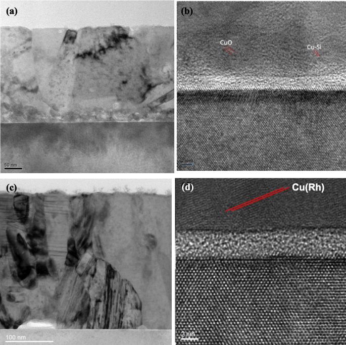
The cross-section TEM image of the pure Cu film after annealing at 400 °C is shown in Fig. 2(a) [9]. A magnified portion of Fig. 2(a) is shown in Fig. 2(b), where we observe the existence of oxidation-resulted CuO and Cu-Si compounds, which conforms to the result of Fig. 1(c) [9]. The cross-section TEM image of the new film after annealing at 670 °C is shown in Fig. 2(c) and magnified in Fig. 2(d). From Fig. 2(d), we observe an Rh phase having a 2.19 Å d-spacing dissolved in the Cu alloy film that not only increases the alloy film’s high-temperature thermal stability but also suppresses oxidation and the intra-reaction between Cu and Si after the crystal grain size has increased to 61 ± 2 nm via annealing.
The (a) TEM image of pure Cu film after having been annealed at 400 °C, (b) the high-resolution TEM of a [9], (c) the TEM image of the new film after having been annealed at 670 °C, and (d) the high-resolution TEM of c
During the optimization processes of the new films, we continuously adjust the added Rh amounts and, after annealing at 400 °C, measure the resulted-in resistivity variations respectively. The experimental results indicate that the resistivity range of the tested films lies at 2.53–4.32 μΩ cm, where the film containing 0.3 at.% Rh composition exhibits the lowest resistivity, 2.53 μΩ cm. The new films tested through the present study, hence, all adopt this (nearly) optimal composition.
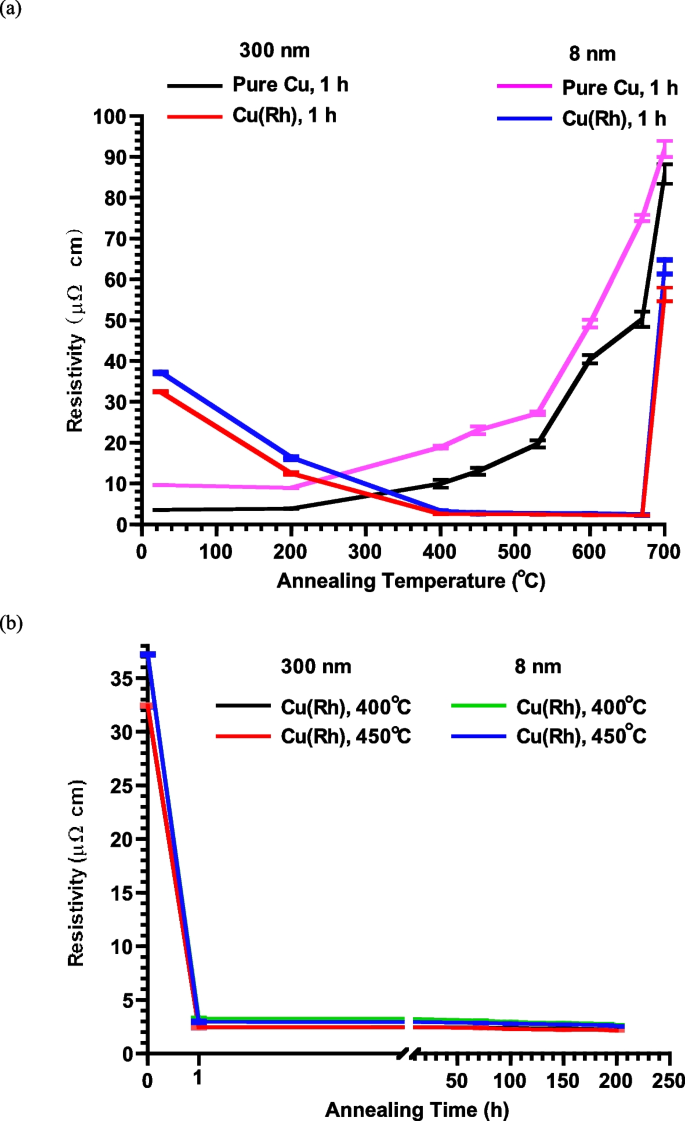
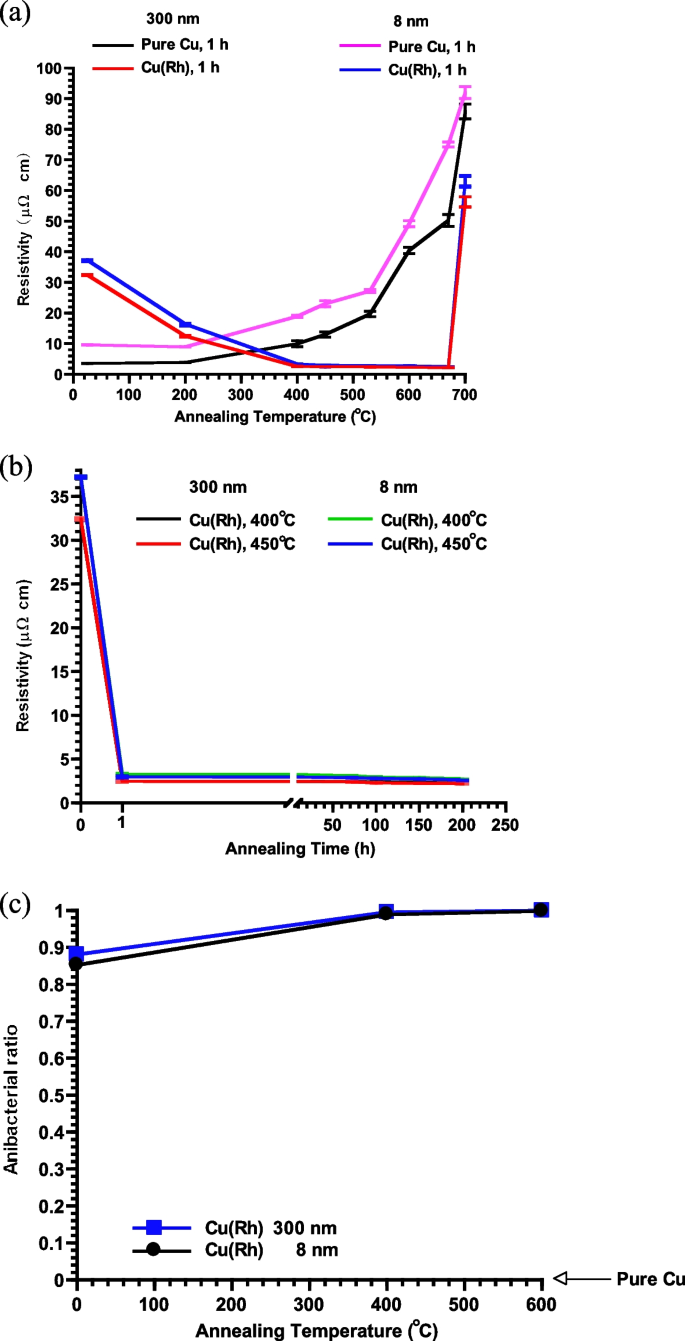
We then anneal the films within a vacuum using annealing temperatures ranging from 400 to 670 °C, resulting in resistivity variations of 2.19, 2.26, and 2.14 μΩ cm, respectively, for the 300-nm-thick Cu(Rh) films that have been annealed at 670 °C for 1 h (Fig. 3(a)) and then 400 and 450 °C for 200 h (Fig. 3(b)). The results conform with the high-temperature anti-oxidation stability of the new film.
a The resistivity variations of pure Cu and Cu(Rh) films (300 nm and 8 nm) deposited on barrierless Si substrates and having been annealed at various temperatures for 1 h, and b the resistivity variations of Cu(Rh) films (300 nm and 8 nm) having been annealed at 400 °C and 450 °C respectively for various time length, up to 200 h
For a Cu(Rh) film annealed at 670 °C for 1 h, the resistance of the 0.3 at.% film is 2.19 μΩ cm. For films with less than 0.3 at.%, specifically 0.2 at.% and 0.1 at.%, the resistances are 2.37 µΩ cm and 2.41 µΩ cm, respectively. In contrast, films with more than 0.3 at.%, such as 0.5 at.% and 0.7 at.%, exhibit higher resistances of 2.6 µΩ cm and 2.8 µΩ cm, respectively. Therefore, the 0.3 at.% film has the lowest resistance value.
Prior to annealing, the Rh phase is supersaturated and solid-soluble in the Cu matrix. Following annealing, the Rh phase precipitates from the Cu matrix grain boundaries owing to stress release, grain growth, and segregation. Therefore, the Cu peak after annealing becomes sharper. This can be determined using XRD (the Rh phase is supersaturated and solid-soluble in the Cu matrix) and high-resolution TEM (grain growth after annealing). Post-annealing resistance measurements reveal a decrease in resistance, aligning with the observed phenomenon.
The XRD analysis in Fig. 1 and the TEM results in Fig. 2 confirm that copper oxide will be generated after annealing pure copper. The increase in resistance observed in Fig. 3 indicates that copper oxide formation increases resistance, adversely affecting the stability of electronic components. After annealing the Cu(Rh) copper alloy film, no copper oxide forms, as evidenced by the low resistance value in Fig. 3. This demonstrates that the Rh phase inhibits copper oxidation, resulting in low resistance, making it suitable for use in copper interconnect and copper alloy seed layers.
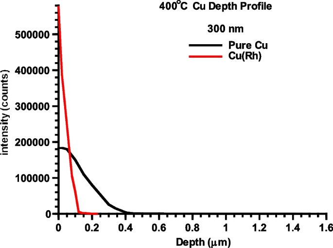
Next, we remove the surface layer of the Cu and Cu alloy films with nitric acid and measure their copper scatter depth with SIMS. The SIMS depth profiles of the pure Cu and Cu(Rh) films after annealing of 400 °C are shown in Fig. 4, where the greatest Cu scattering depth of the new film is approximately 0.22 μm, which is much lower than that of 0.42 μm for its pure Cu counterpart [9]. This finding further verifies that the high-temperature thermal stability of the new film is superior to that of a pure Cu film.
The SIMS Cu depth profile (300 nm thick) of the pure Cu [9] and Cu(Rh) alloy films after having been annealed for 400 °C
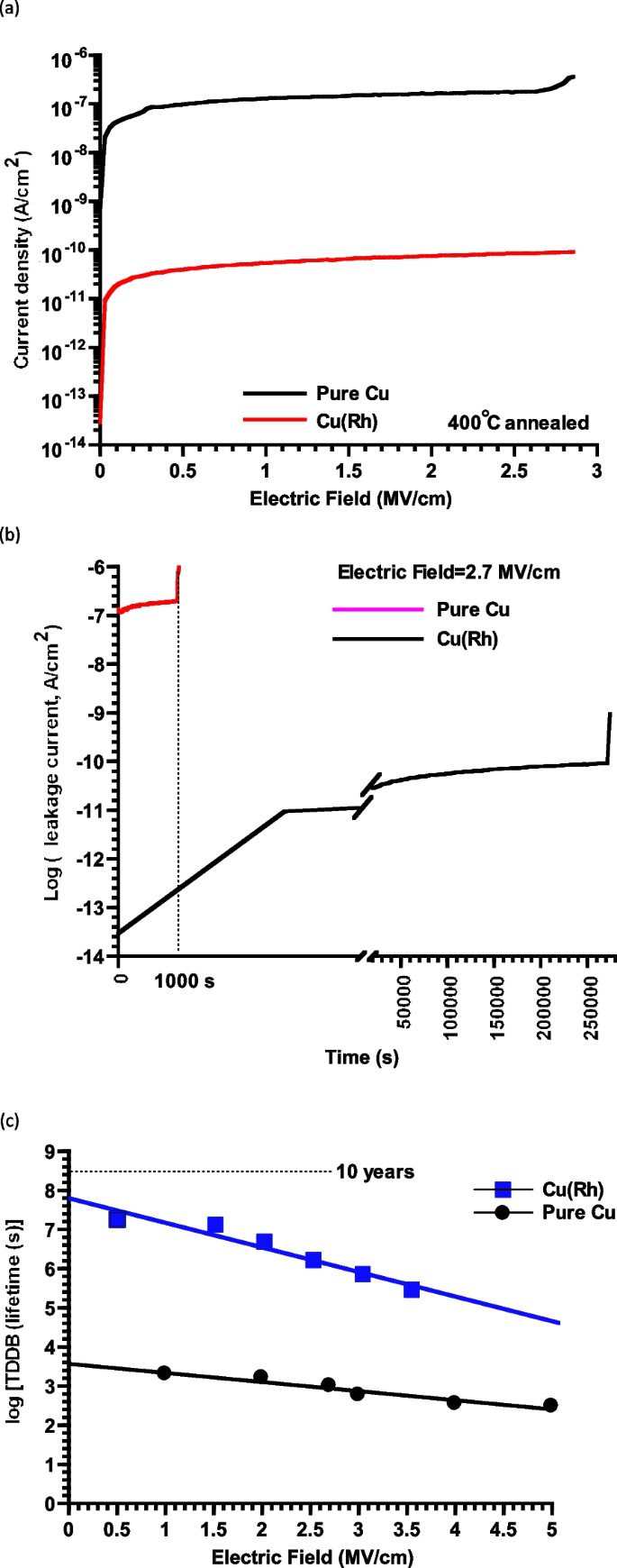
The I–V curves of the formed metal–oxide–silicon (MOS) capacitors, which are made by co-sputtering Cu and Cu(Rh) onto SiO2/Si substrates and annealed for 1 h, are shown in Fig. 5(a). The annealing temperature is set at 400 °C for high-temperature evaluation [25]. When electric field strength exceeds 2.7MV/cm, the leakage current of the capacitors’ pure Cu gates rises owing to some Cu substance that is scattered into SiO2 during the annealing process. When the electric field strength is set at 2 MV/cm, the leakage current of the new film (7.53 × 10⁻¹¹ A/cm2) is lower than that of Cu(NbZr) [11] (1.43 × 10⁻¹⁰ A/cm2), that of Cu(RuNx) [15] (3.17 × 10⁻¹⁰ A/cm2), that of Cu(RuHfNx) [16] (1.83 × 10⁻¹⁰ A/cm2), and that of pure Cu (1.6 × 10⁻⁷ A/cm2) [9], indicating that the new film holds high-temperature thermal stability and is a good candidate material for barrierless layers. This result conforms to the SIMS test results shown in Fig. 4. The I–V curves of two types of capacitors stressed at 2.7MV/cm are shown in Fig. 5(b). As time passes by, the ion thickness and the number of electric charges captured and accumulated in the oxidation layer will cause the leakage current to increase abruptly, resulting in structural damage. To a pure Cu film [9] and the new film, a leakage current will penetrate through the oxidation layer and damage the structure once the ion thickness at the SiO2/Si interface reaches their critical thresholds after 1000 s and 274,200 s, respectively. Under 2.7 MV/cm, the time the new film takes to arrive, structural damage is much longer than, and hence superior to, the pure Cu [9] and some other Cu alloy films, which indicates that the new film’s electric reliability is higher. The relationship between the films’ TDDB lifetime and the electric field strength is shown in Fig. 5(c), where the new film’s time to failure concerning the applied stress voltage satisfies 10-year projected reliability. The new film’s TDDB lifetime under 3.5 MV/cm is substantially longer than that of the pure Cu film, i.e., 63,095,734 s for the former and 3981 s for the latter, a 15,849-fold difference. While the new film’s high-temperature thermal stability confirms that the new film, TiN [26], Ta [26], and the barrier layer of TaN [26] are all thermally stable, the exceptional outcome of the new film’s TDDB lifetime (> 10 years) makes Cu(Rh) a highly desirable circuit-printing interconnect material.
The I–V (i.e., current-votlatge) curves of MOS capacitors formed by (a) the pure Cu [9] and Cu(Rh) films deposited on SiO2/Si substrates and then annealed at 400 °C for 1 h, (b) the MOS capacitors’ leakage current under 2.7MV/cm electric field stress, and (c) the relationship between electric field strength and TDDB lifetime for the pure Cu [9] and Cu(Rh) film (300 nm thick)
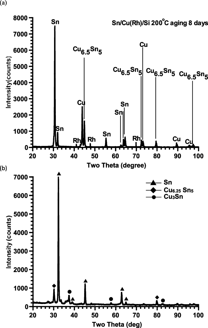
The XRD analysis result of an Sn/Cu(Rh)/Si structure after aging for 8 D is shown in Fig. 6(a). Although the Cu–Sn intermetallic compound is incurred, the Cu(Rh) buffer layer still exists in the alloy film without reacting with Sn. The result confirms the chemical stability of Cu(Rh). In comparison, after aging for 8 D, the Sn/Cu/Cr/Si structure not only preserves no more pure Cu by XRD analysis [13] but also is converted into Cu–Sn metal compounds. I hence deduce that the Rh within Cu(Rh) has improved the new film’s stability during the Cu-Sn aging period.
The XRD pattern of an Sn/Cu(Rh)/Si structure (a) having been annealed at 200 °C for 8 D (i.e., days), and (b) the XRD pattern for an Sn/Cu/Cr/Si structure having been annealed at 200 °C for 8 D [13] (300 nm thick)
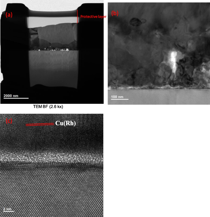
The TEM images of the Sn/Cu(Rh)/Si structure after having been annealed at 200 °C for 8 D are shown in Fig. 7(a)–(c), where c is the magnified TEM image of b. Figure 7(c) displays that a 2.19 Å d-spacing of the Rh phase exists in the new alloy, conforming with the XRD patterns of Figs. 1(a) and (c). This, again, verifies that the buffer of Cu(Rh) possesses both high thermal stability and Cu–Sn-reaction suppression capability.
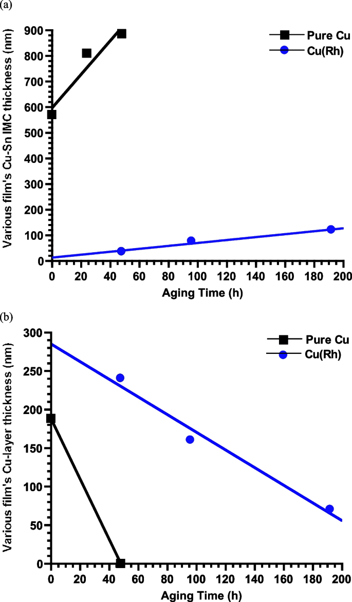
The thickness of the new film’s Cu–Sn IMC layer before and after annealing is less than that of the pure Cu film, as shown in Fig. 8(a). As the aging starts, the pure Cu [13] film’s IMC layer thickness is approximately 600 nm while that of the new film is approximately 5 nm, way below the former. Their difference in IMC-layer thickness widens as the aging process continues. From Fig. 8(b), we observe that after aging for 8 D, the new Cu(Rh) film still retains a 70-nm-thick Cu layer while, in comparison, that Cu layer within the pure Cu film has fully been dissipated and disappears after aging for 2 D. This indicates that Cu(Rh) is a very stable material. The addition of approximately 3 at. % Rh to Cu to effectively inhibit the formation of intermetallic compounds at the film-substrate interface, as proposed and achieved in the present study, has not been reported in the literature to date. This is a contribution to the material science and the applied material industries. The exact mechanism of this phenomenon is still not fully clear; further studies are suggested.
a The thickness of a Cu–Sn layer, grown at 200 °C on Cu [13], and Cu(Rh) film, as a function of reflow time. b The thickness of the new film after thermal aging at 200 °C for different periods
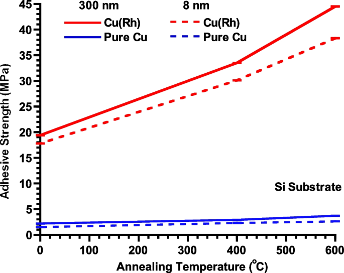
The adhesive strength measurements, via ASTM D4541-02 adhesion test, on pure Cu films and the new films (8 and 300 nm thick) are shown in Fig. 9, where the films deposited on barrierless Si substrates are as deposited or as having been annealed at 600 °C for 1 h. As for the 300-nm-thick films, the new alloy film’s adhesive strength on a Si-substrate before annealing, 19.1 ± 0.02 MPa, is approximately 9 ~ tenfold of that of its pure Cu counterpart. After annealing, the new film’s adhesive strength rises to 44.2 ± 0.01 MPa, approximately 11–12 folds of that of its pure Cu counterpart, viz. 3.7 ± 0.02 MPa. This is similar to the earlier adhesive strength comparison result of Cu(RuNx) vs. pure Cu films [15]. I deduce that the greater adhesive strength of the new alloy film may be attributed to the Rh that is segregated to the film-Si interface. The theory still needs further verification.
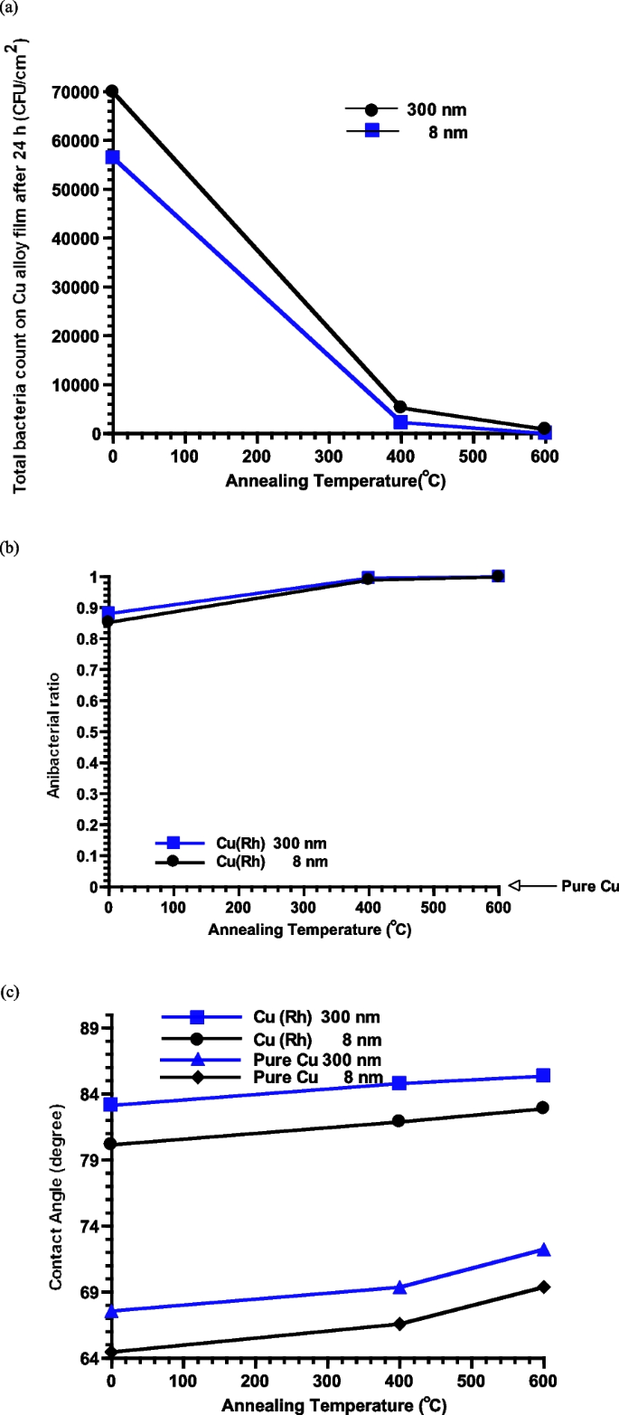
Having been exposed to S. aureus BCRC 10451 bacteria for 24 h, the pure Cu and new films (8 and 300 nm thick), which are as deposited or have been annealed at various temperatures, exhibit various degrees of antibacterial efficacy. Figure 10(a) shows the films’ bacteria count, (b) their antibacterial ratio, and (c) their contact angle. From Fig. 10(a and b), the antibacterial efficacy of the new 300-nm-thick film, after having been annealed at 600 °C for 1 h, seems excellent, with an antibacterial ratio of approximately 100%. Reducing the new film’s thickness to 8 nm, which has undergone the same annealing process, an antibacterial ratio of approximately 99.82% still can be reached. These are far superior to the antibacterial ratio of their pure Cu counterpart, which is always 0 via any annealing temperatures. Figure 10(c) depicts the contact angle variations of the films after having been annealed at various temperatures. Before annealing, the crystal grain sizes are relatively small, 17 ± 3 nm, so the films are not that tight and compact, and the contact angles are relatively smaller. After annealing, the grain sizes have grown to 58 ± 2 nm, resulting in a more compact film structure and larger contact angles. The smaller the angles are, the gluier the bacteria to the films are, and vice versa. From this figure, we observe that after the new film is annealed, its contact angles become greater, with its Rh phase affecting its surface tension, leading to the greatest antibacterial efficacy. When the film thickness is reduced to 8 nm, the incurred negative effect toward the efficacy is still the least for the new film, which indicates the superior antibacterial stability of the new film. This conforms with the test results shown in Fig. 10(b) and is consistent with an earlier result conducted by the author on Cu(NbC) films [27].
The antibacterial efficacy comparison among pure Cu [27] and the new alloy (8 and 300 nm thick) films, as-deposited and after annealing at various temperatures, with the films having been exposed to S. aureus BCRC 10451 bacteria for 24 h, where a comparison in bacteria count, b in antibacterial ratio, and c in contact angle
The previously mentioned factors all seem to indicate that the new film comparatively possesses merits and superiority for industrial and antibacterial applications.
4 Conclusion
A new type of Cu(Rh) films developed in the study via the co-sputtering method and various annealing processes exhibits remarkable characteristics, such as low resistivity, high-temperature thermal stability, flip-chip solder joint stability, great adhesive strength, long TDDB lifetime, and high antibacterial efficacy. A 0.3 at. % Rh composition is used throughout the study to provide (nearly) the lowest resistivity after many trial-and-error experiments.
Related tests are conducted with the results revealed in detail herein. After analyzing the test results, the new film appears to be a significant candidate material for various industrial applications, including ultra-large integrated circuits, micro-electronic circuits, printed circuits, flip-chip technology, wafer-level chip-scale packaging, and antibacterial use, and the like.
Availability of data and materials
The authors confirm that the data supporting the findings of this study are available within the article.
References
-
S.K. Kang, D.Y. Shih, K. Fogel, L.P. Di, Interfacial reaction studies on lead (Pb)-free solder alloys, IEEE Trans. Electron. Packag. Manuf. 25, 155–161 (2008)
-
C.E. Ho, C.R. Kao, Interfacial reaction issues for lead-free electronic solders. J. Mater. Sci.: Mater. Electron. 18, 155–174 (2007)
-
J.G. Lozano, S. Lozano-Perez, J. Bogan, Y.C. Wang, B. Brennan, P.D. Nellist, G. Hughes, Interdiffusion and barrier layer formation in thermally evaporated Mn/Cu heterostructures on SiO2 substrates. Appl. Phys. Lett. 98, 123112 (2011)
-
S.M. Rossnagel, T.S. Kuan, Alteration of Cu conductivity in the size effect regime. J. Vac. Sci. Technol. B 22, 240–247 (2004)
-
J.P. Chu, C.H. Lin, High performance Cu containing Ru or RuNx for barrierless metallization IEEE Int. Interconnect Technology Conference, 2008. IITC 2008. International (Burlingame USA, 2008), p. 25
-
C.-H. Lin, H.-Y. Chuang, C.R. Kao, Cu(TiWNx) Film as a barrierless buffer layer for metallization applications. Jpn. J. Appl. Phys 52, 01AC12 (2013)
-
C.H. Lin, A new copper alloy film for barrierless Si metallization and solder bump flip-chip application. Jpn. J. Appl. Phys. 52, 05FB01 (2013)
-
H.-Y. Chuang, C.H. Lin, J.P. Chu, C.R. Kao, Novel Cu–RuNx composite layer with good solderability and very low consumption rate. J. Alloys. Compd. 504, L25–L27 (2010)
-
C.H. Lin, J.P. Chu, T. Mahalingam, T.N. Lin, S.F. Wang, Thermal stability of sputtered copper films containing dilute insoluble tungsten: Thermal annealing study. J. Mater. Res. 18, 1429–1434 (2003)
-
C.-H. Lin, A new Cu(NbCNx) film and some of its characteristics. Microelectron. Eng. 223, 111217 (2020)
-
L. Chon-Hsin, Newly-developed Cu(NbZrNx) copper-alloy films for microelectronic manufacture advancement. Mater. Trans. 63, 1080–1086 (2022)
-
C.-H. Lin, New Cu(TiBNx) copper alloy films for industrial applications. Jpn. J. Appl. Phys. 55, 06JD02 (2016)
-
C.-H. Lin, New Cu(AuTiNx) copper alloy film and its features. Jpn. J. Appl. Phys. 55, 01AA13 (2016)
-
J.P. Chu, C.H. Lin, P. Sun, L, and Leau W. K., Cu (ReNx) for advanced barrierless interconnects stable up to 730° C. J. Electrochem. Soc. 156, H540 (2009)
-
J.P. Chu, C.H. Lin, V.S. John, Cu films containing insoluble Ru and RuNX on barrierless Si for excellent property improvements. Appl. Phys. Lett. 91, 132109 (2007)
-
C.H. Lin, W.K. Leau, C.H. Wu, The application of barrierless metallization in making copper alloy, Cu(RuHfN), films for fine interconnects. Electron. Mater. 39, 2441–2447 (2010)
-
C.H. Lin, W.K. Leau, Copper-silver alloy for advanced barrierless metallization. Electron. Mater. 38, 2212–2221 (2009)
-
CAS #: 7440–16–6, https://www.americanelements.com/rhodium-metal-7440-16-6
-
C.B. Cheng, C. Hongmei, A. Isaac, W. Jiheng, Z. Yilin, W. Jun, J. Feiran, W. Ze, Y. Shui, W. Lei, J. Lei, Q. Yanxin, Self-formed diffusion layer in Cu(Re) alloy film for barrierless copper metallization. Coatings 12, 613 (2022)
-
S. Hanna, A. Oscar, R.R. Johnson, P.V. Palmieri, Co-sputtered amorphous Nb–Ta, Nb–Zr and Ta–Zr coatings for corrosion protection of cyclotron targets for production. J. Alloy. Compd. 639, 488–495 (2015)
-
M. André, H. Susanne, T. Ladji, G. Gregor, B. Jörg, H. Nies Dietrich, Survival of bacteria on metallic copper surfaces in a hospital trial. Appl. Microbiol. Biotechnol. 87, 1875–1879 (2010)
-
S.C. Espírito, L.E. Wen, C.G. Elowsky, Q. Davide, D.W. Domaille, C.J. Chang, G. Gregor, Bacterial killing by dry metallic copper surfaces. Appl. Environ. Microbiol. 77, 794–802 (2011)
-
L. Zeming, J.E. Stout, T. Lou, B. Marcie, H. Charles, W.F. Diven, V.L. Yu, Controlled evaluation of copper-silver ionization in eradicating Legionella pneumophila from a hospital water distribution system. J. Infect. Dis. 169, 919–922 (1994)
-
JIS Z 2801 Test method
-
K. Barmak, C. Cabral Jr., K.P. Rodbell, J.M.E. Harper, On the use of alloying elements for Cu interconnect applications. J. Vac. Sci. Technol. B 24, 2485–2498 (2006)
-
G. Soto, A. Rosas, M.H. Farias, W. De la Cruz, J.A. Diaz, Characterization of rhenium nitride films produced by reactive pulsed laser deposition. Mater. Charact 58, 519–526 (2007)
-
C.-H. Lin, Some aspects of new Cu(NbC) films. Bull. Mater. Sci. 43, 1 (2020)
Acknowledgements
The author thanks Dr. John Yanhao Chen, who is with eWay Inc. in Taiwan, for his invaluable discussions and advice for this paper.
Funding
This work was sponsored by the National Science Council of the Republic of China in Taiwan, under Project No. 106–2221-E-243–001-MY3-.
Author information
Authors and Affiliations
Contributions
This paper is in charge of Dr. Chon-Hsin Lin which include 1. Conceptualization 2. Methodology 3. Validation 4. Formal analysis 5. Investigation 6. Resources 7. Data Curation 8. Writing - Original Draft 9. Writing - Review & Editing 10. Visualization 11. Supervision 12. Project administration 13. Funding acquisition.
Corresponding author
Ethics declarations
Competing interests
The author declares no competing interests.
Additional information
Publisher's Note
Springer Nature remains neutral with regard to jurisdictional claims in published maps and institutional affiliations.


