Vol.32 (Apr) 2022 | Article no.9 2022
We investigate the growth and electronic properties of the Sn sheets on Cd(0001) with a low-temperature scanning tunneling microscopy (STM) and density functional theory (DFT) calculations. It is found that both the first and second layer of Sn reveal the epitaxial growth with a 1 × 1 commensurate lattice. Scanning tunneling microscopy (STS) measurements indicate the Sn monolayer exhibits a metallic behavior. DFT calculations indicate that all the Sn atoms in the first Sn layer occupy the energetically preferable hcp-hollow sites. Very small amount of charge is transferred from Cd(0001) to the Sn monolayer, indicating the interface of Sn/Cd(0001) is governed by the weak van der Waals interaction.
Tin (Sn) is a peculiar element within the carbon group of the periodic table. It has two allotropic forms: gray Sn (α-Sn) and white Sn (β-Sn). At room temperature (RT), β-Sn is a stable metallic phase with body-centered tetragonal structure. It shows novel physical properties such as superconductivity and quantum-well states (QWS) [1,2,3,4,5,6]. When temperature is below 13.2 °C, β-Sn undergoes a phase transition into the semiconducting α-Sn with a diamond structure.
Stanene is a single layer of α-Sn(111) with honeycomb structure, similar to the well-known graphene. First-principle calculations predicated that stanene and its derivatives could serve as a promising two-dimensional (2D) topological insulator to realize the RT quantum spin Hall (QSH) effect [7]. Moreover, the stanene-based 2D materials possess extraordinary properties such as topological superconductivity, giant magnetoresistance, and enhanced thermoelectric performance [8,9,10,11]. These theoretical studies stimulated the extensive studies on the experimental synthesis of various stanene sheets. In 2015, the JIA Group reported a novel stanene layer grown on Bi2Te3(111) by molecular beam epitaxy (MBE) [12]. Subsequently, a series of stanene sheets were successfully fabricated on various substrates such as PbTe(111) [13], InSb(111) [14, 15], Sb(111) [16], Cu(111) [17], Bi(111) [18], Au(111) [19,20,21], and Ag(111) [22]. Especially, the ultraflat stanene formed on Cu(111) reveals a topologically edge state with a sizeable gap of 0.3 eV [17]. Previously, theoretical studies also predicted a metastable Sn allotrope with face-centered cubic structure (fcc-Sn) [23, 24]. Recently, the JIA Group observed the fcc-Sn on the superconductive 2H-NbSe2(0001) surface and demonstrated its metastability [25].
Sometimes surface alloying occurs when Sn atoms are deposited on metal surfaces at RT. For instance, when adsorbed on Cu(001) surface at RT, Sn atoms form five different Cu-Sn alloy phases: p(2 × 2), p(2 × 6), c(4 × 8), p(3√2 × √2)-R45°, and c(4 × 4) [26]. Similarly, Sn on Cu(111) may form a stable 2D alloy phase with p(√3 × √3)-R30° structure at or above RT [27, 28].
In this paper, we choose the divalent hexagonal close-packed metal Cd(0001) thin films as substrates to grow the epitaxial stanene. Compared to the noble metals Au, Ag, and Cu, the metal Cd has a smaller electronegativity and a negative electron affinity [29,30,31]. Thus charge transfer effect is expected to be very weak between the Sn atoms and Cd(0001) films. It is observed that low-temperature deposition of Sn atoms on Cd(0001) at ~100 K leads to the epitaxial growth of stanene sheet with 1 × 1 commensurate structure. Scanning tunneling spectrum (STS) measurements disclose that the first monolayer Sn exhibits a metallic behavior. Density function theory (DFT) calculations indicate that the hcp-hollow site of Cd(0001) is the most energetically favorable site of Sn atoms.
Our experiments were carried out in an ultrahigh vacuum Unisoku LT-STM system with a base pressure of 2.0 × 10⁻¹⁰ torr. Firstly, the Cd(0001) thin films were prepared by depositing ten monolayers of Cd atoms onto a Si(111)-7 × 7 surface at RT. Then, high-purity tin (99.999 %) was thermally evaporated onto the Cd(0001) surface from a quartz crucible heated to 750 °C. The deposition rate is around 0.1 monolayer per minute. Here, we define one monolayer of Sn in terms of the atom density of Cd(0001) surface. During the deposition, the Cd(0001) substrate was kept at ~100 K, and the pressure was maintained at 3.0 × 10⁻⁹ torr. After deposition, the sample was immediately transferred into the LT-STM chamber (77.8 K). An electrochemically etched tungsten tip was cleaned by electron beam heating.
DFT calculations were performed by the Quantum ESPRESSO package [32]. We calculated the geometric and electronic structures by using the generalized gradient approximation (GGA) of Perdew-Burke-Ernzerhof formula and the optimized norm-conserving Vanderbilt pseudopotentials [33, 34]. The slab was constructed by a Sn monolayer and six Cd atomic layers. A vacuum layer of 20 Å was inserted to avoid the coupling between atomic layers along the c axis. A 5 × 5 unit cell is constructed so as to describe the hexagonal Sn monolayer on Cd(0001) surface. After the convergence test, the kinetic-energy cutoff and the charge-density cutoff were chosen to be 60 and 480 Ry, respectively. The charge densities were calculated on an unshifted mesh of 17 × 17 × 2 points in combination with a Marzari-Vanderbilt smearing of 0.02 Ry [35]. The geometry optimization was performed until all components of all forces became less than 1.0 × 10⁻³ eV·Å−1. Based on the optimized structure, we performed density of states (DOS) calculations.
Figure 1a shows the morphology of the as-grown Cd thin films with large and smooth terraces. It can be seen from the height profile line in Fig. 1b; the Cd films reveal a step height of 2.8 ± 0.1 Å, in a perfect agreement with the interlayer spacing of bulk Cd at 0001 direction [36]. From the atomic-resolution STM image in Fig. 1c, the in-plane structure of Cd film reveals a hexagonal lattice constant of c0 = 3.0 ± 0.1 Å, also consistent with that of (0001) plane of bulk Cd. Hence, the Cd film grown on Si(111)-7 × 7 corresponds to a crystalline Cd(0001) thin film. Figure 1d shows the atomic model of the Cd(0001) films, where the four high-symmetric sites are emphasized by F (fcc-hollow), H (hcp-hollow), B (bridge), and T (top), respectively.
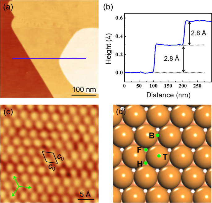
a Morphology of the Cd(0001) thin film grown on a Si(111)-7 × 7 surface (U = 2.0 V, I = 20 pA). b Height profile along the blue line in (a) showing the step height of 2.8 A. c High-resolution STM image of the Cd(0001) thin film showing a hexagonal lattice (U = 0.15 V, I = 22 pA). d Atomic model of the Cd(0001) surface. Orange and light red balls represent Cd atoms in the first and second layer, respectively. The high-symmetric sites are emphasized by F (fcc-hollow), H (hcp-hollow), B (bridge), and T (top)
We deposit firstly 0.3 mL of Sn atoms onto the Cd(0001) surface at low temperature (~100 K). As shown in Fig. 2a, Sn atoms form a series of 2D islands with several tens of nanometers in size. There are some small Sn clusters decorated at the island edges. From the profile line in Fig. 2b, it is found that the Sn island reveals an apparent height of 2.7 Å, which is slightly lower than the atomic step height (2.8 Å) of Cd(0001). When the Sn coverage is increased to 0.6 mL, the individual Sn islands grow up laterally and coalesce into larger 2D islands with hundreds of nanometers in size (Fig. 2c). Meanwhile, the small decorated Sn clusters grow into the second layer islands. In principle, the formation of second layer islands in the submonolayer regime implies a sizeable Ehrlich-Schwoebel barrier at the step edges [37,38,39]. Figure 2d shows a high-resolution STM image of the first Sn layer. It is observed that the Sn atoms reveal a hexagonal lattice with the periodicity c = 3.0 ± 0.1 Å, which is coincident with that of Cd(0001). Furthermore, the lattice orientations of Sn monolayer run parallel to the high symmetry directions of Cd(0001), demonstrating the perfect 1 × 1 commensurate epitaxy of the first Sn layer. In Reference [25], the fcc-Sn(111) on NbSe2 revealed a lattice constant of 0.35 nm, which is 17% larger than that of the 1 × 1 commensurate phase observed here. On the other hand, both the two structures have the nearly same interlayer spacing (0.27 nm) at the vertical direction.
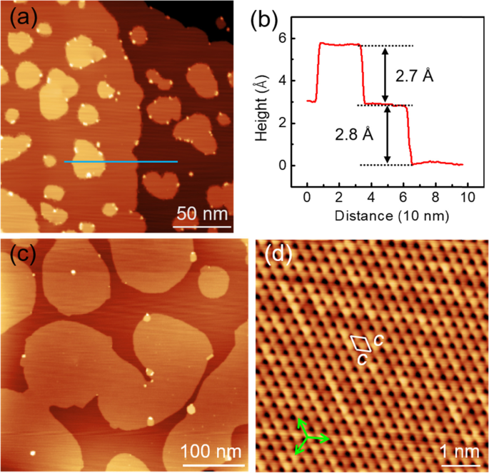
a STM image of the 2D Sn islands formed on Cd(0001) at 0.3 ML (U = 2.5 V, I = 20 pA). b A line profile along the blue line in (a), showing the different heights of 2D Sn islands and substrate steps. c Coalescing of the 2D Sn islands into large islands with hundreds of nanometers in size, when the Sn coverage is increased to 0.6 ML (U = 2.0 V and I = 20 pA). d Atomic-resolution STM image of the Sn monolayer, showing the hexagonal lattice with a periodicity of 3.0 A (0.6 V, 25 pA). The unit cell is labelled by a white rhombus
When the Sn coverage is increased to 1.2 mL, almost the entire surface of Cd substrate is covered by the Sn monolayer. Meanwhile, the small second layer islands can be observed on top of the first Sn layer (Fig. 3a). Like the first Sn layer, the second Sn layer also has an apparent height of 2.7 A. Figure 3b shows a high-resolution STM image of the second Sn layer. It can be seen that the second Sn layer also reveals a hexagonal lattice with a periodicity of 3.0 A, the same as that of the first Sn layer. Thus, we conclude that the epitaxial growth of Sn films can persist up to two monolayers. Similar to the small clusters in the submonolayer regime (Fig. 2a), there are some small bright protrusions appeared at the island edges of the second Sn layer (Fig. 3a), which correspond to the nucleation of the third Sn layer. Based on the morphology of the first and second Sn layers, as well as the small clusters on top of the second Sn layer, the Stranski-Krastanov mode can be identified for the growth of Sn sheet on Cd(0001).
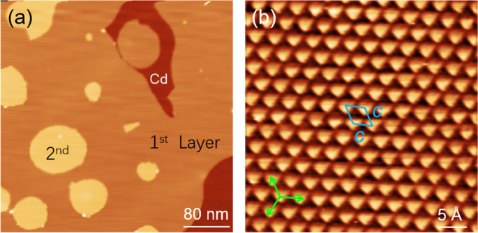
a Topography of the Sn sheet formed at 1.2 ML (U = 2.0 V, I = 20 pA). b Atomic-resolution STM image of the second layer of Sn sheet (U = 0.8 V, I = 20 pA), showing the same hexagonal lattice as the first Sn layer
In order to explore the electronic structure of the Sn monolayer, we perform the STS measurements on top of a round Sn island with a diameter of 48 nm (Fig. 4a). Shown in Fig. 4b are two differential conductance spectra taken at the island center (A) and island edge (B) positions, respectively. Apparently, the two dI/dV spectra look very similar with their peaks appeared at the same energy positions. The only difference between the two spectra lies at the intensity of differential conductance. Thus, it means that the topological edge state does not exist in the first Sn layer. Furthermore, the nonzero conductance at the position of Fermi energy indicates the metallic nature of the first Sn layer.
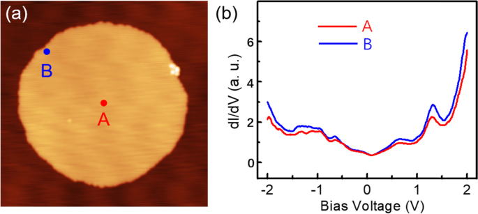
a A 2D Sn island formed on the Cd(0001) surface (U = 0.6 V, I = 21 pA ). b Two dI/dV spectra (setpoint U = 0.4 V, I = 150 pA) acquired at the island center (A) and island edge (B), respectively
To get insight into the experimental results, we carried out DFT calculations on the monolayer Sn on Cd(0001). The adsorption energy (Eads) was used to evaluate the adsorbate-substrate interaction. Here, Eads is defined as the mean adsorption energy per adatom,
where Esn/Cd(0001) and ECd(0001) are the total energy of the Cd(0001) system after and before Sn atoms adsorption, respectively, n represents the number of adatom, and ESn is the energy of an isolated Sn atom. Here, a negative adsorption energy corresponds to the exothermic process. In order to find the most stable structure of Sn monolayer, we considered four typical adsorption sites: the top, bridge, hcp-hollow, and fcc-hollow sites. After full geometry optimizations, the calculated Eads and main geometrical parameters are summarized in Table 1. It is found that all the four adsorption energies are negative. In particular, the hcp-hollow site is found to be the most energetically preferred site for Sn atom on Cd(0001) due to the adsorption energy of −0.202 eV per Sn atom. Figure 5a shows the top view of the optimized structural model of Sn monolayer on Cd(0001), in which all the Sn atoms occupy the hcp-hollow sites. The calculated Sn–Sn bond length (dSn-Sn = 0.2989 nm) and the adsorption height (0.302 nm) are close to the experimentally observed 1 × 1 commensurate structure (dSn-Sn = 0.30 nm, dSn-Cd = 0.27 nm). We also found that the calculated Sn–Sn bond length is close to that of Sn crystals (0.31 nm in β-Sn and 0.288 Å in α-Sn) as well as the average neighbor distance in Sn nanoclusters [40,41,42,43,44,45].
| Sites | Eads (eV) | dSn-Cd (nm) | dSn-Sn (nm) |
|---|---|---|---|
| Top | –0.176 | 0.3187 | 0.2989 |
| Bridge | –0.199 | 0.3032 | |
| Hollow-fcc | –0.197 | 0.3024 | |
| Hollow-hcp | –0.202 | 0.3020 |
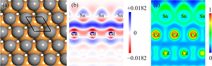
a The optimized configuration of monolayer Sn on the Cd(0001) surface. The gray and orange balls represent Sn and Cd atoms, respectively. The black rhombus represents the unit cell. b Side view of the charge density difference of the Sn/Cd(0001) system. The charge accumulation and depletion are indicated by blue and red colors, respectively. c Side view of the electron localization function (ELF) in the Sn/Cd(0001) system
We also analyzed the electronic structure of the optimized Sn monolayer on Cd(0001) in terms of charge density difference (Δρ) and electron localization function (ELF). The ELF reflects the localization of electrons in a crystal structure and is defined as follows:
where the φi and ρ represent Hartree-Fock or Kohn-Sham orbitals, the distribution of electron density, respectively. As shown in Fig. 5b, the charge accumulation and depletion are indicated by blue and red colors, respectively, while the white color indicates the unchanged charge density. It can be seen that the charge accumulation appears mainly in the interface region between Sn and Cd atomic layer due to the influence of surface effect. The total amount of charge transfer is 0.0182 e from Cd(0001) to Sn monolayer. The ELF can directly allow one to evaluate chemical interactions from the charge localization between individual atoms. The value of ELF is limited between 0 and 1, where 1 represents the highly localized electrons, 0.5 indicates electron-gas-like pair probability, and 0 corresponds to electrons without localization [46]. Figure 5c shows the side view of ELF pattern in the Sn/Cd(0001) system, where an ELF value of ~0.4 can be derived for the Sn–Sn pair. In contrast, very small ELF value (~0.2) appeared in the region between the Sn atom and the topmost Cd atoms. Therefore, it can be concluded that both the Sn–Cd or Sn–Sn interactions are mainly of an electrostatic origin, but the former is weaker than the latter. In addition, the interlayer distance between Sn monolayer and Cd(0001) is 3.02 Å, which is significantly larger than the Sn–Cd bonding distance (2.6758 Å) [47], indicating that the interaction between Sn monolayer and the Cd(0001) is weak van der Waals (vdW) interaction.
Figure 6a shows the comparison between the calculated local density of states (LDOS) and the experimental dI/dV spectrum. It is found that calculated LDOS resembles the measured STS spectrum. In particular, the LDOS peaks far from the Fermi level are coincident with the STS peaks, indicating the optimized structural model for monolayer Sn on Cd(0001) is reasonable. Thus, we conclude that the interaction between Sn and Cd(0001) is governed by the weak van der Waals interaction, and no chemical bonding existed at the interface of Sn/Cd(0001).
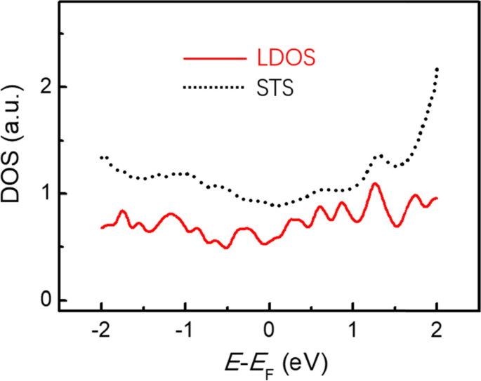
Comparison between the calculated local density of states (LDOS) (red) of the Sn monolayer with the experimental dI/dV spectra (dotted black) acquired on top of the Sn monolayer
To summarize, we have found the epitaxial growth of a hexagonal monolayer of Sn on the Cd(0001) surface. STS measurements indicate the Sn monolayer reveals a metallic behavior. DFT calculations indicate that all the Sn atoms occupy the energetically preferable hcp-hollow sites. Very small amount of charge transfer (0.0182 e) takes place from Cd(0001) to Sn monolayer, indicating the interface of Sn/Cd(0001) is governed by the weak van der Waals interaction. Moreover, the second Sn layer also exhibits the same hexagonal lattice as the first Sn monolayer. These results are highly relevant to the fabrication of new ultrathin Sn sheets on solid surfaces with novel physical properties.
All data and figures presented in this article are based on the materials available in public through the corresponding references with their permissions.
J.M. Rowell, W.L. McMillan, W.L. Feldmann, Phys. Rev. B 3, 4065 (1971)
V.S. Egorov, G. Solt, C. Baines, D. Herlach, U. Zimmermann, Phys. B 393, 289–90 (2000)
V.S. Egorov, G. Solt, C. Baines, D. Herlach, U. Zimmermann, Phys. Rev. B 64, 024524 (2001)
Z.B. Shao, Z.Y. Zhang, H. Yuan, H.G. Sun, Y. Cao, X. Zhang, S.J. Li, H. Gedeon, T. Xiang, Q.K. Xue, M.H. Pan, Sci. Bull. 63, 1332–1337 (2018)
L.L. Wang, X.C. Ma, S.H. Ji, Y.S. Fu, Q.T. Shen, J.F. Jia, K.F. Kelly, Q.K. Xue, Phys. Rev. B 77, 205410 (2008)
Z.R. Wang, C.X. Zhao, G.Y. Wang, J. Qin, B. Xia, B. Yang, D.D. Guan, S.Y. Wang, H. Zheng, Y.Y. Li, C.H. Liu, J.F. Jia, Chin. Phys. Lett. 37, 096801 (2020)
Y. Xu, B. Yan, H.J. Zhang, J. Wang, G. Xu, P. Tang, W. Duan, S.C. Zhang, Phys. Rev. Lett. 111, 136804 (2013)
J. Wang, Y. Xu, S.C. Zhang, Phys. Rev. B 90, 054503 (2014)
S.C. Wu, G.C. Shan, B.H. Yan, Phys. Rev. Lett. 113, 256401 (2014)
S. Rachel, M. Ezawa, Phys. Rev. B 89, 195303 (2014)
Y. Xu, Z.X. Gan, S.C. Zhang, Phys. Rev. Lett. 112, 226801 (2014)
F.F. Zhu, W.J. Chen, Y. Xu, C.L. Gao, D.D. Guan, C.H. Liu, D. Qian, S.C. Zhang, J.F. Jia, Nat. Mater. 14, 1020–1025 (2015)
Y.Y. Zang, T. Jiang, Y. Gong, Z.Y. Guan, C. Liu, M.H. Liao, K.J. Zhu, Z. Li, L.L. Wang, W. Li, C.L. Song, D. Zhang, Y. Xu, K. He, X.C. Ma, S.C. Zhang, Q.K. Xue, Adv. Funct. Mater. 28, 1802723 (2018)
C.Z. Xu, Y.H. Chan, P. Chen, X.X. Wang, D. Flötotto, J.A. Hlevyack, G. Bian, S.K. Mo, M.Y. Chou, T.C. Chiang, Phys. Rev. B 97, 035122 (2018)
X.H. Zheng, J.F. Zhang, B.B. Tong, R.R. Du, 2D Mater. 7, 011001 (2019)
J. Gou, L.J. Kong, H. Li, Q. Zhong, W.B. Li, P. Cheng, L. Chen, K.H. Wu, Phys. Rev. Mater. 1, 054004 (2017)
J.L. Deng, B.Y. Xia, X.C. Ma, H.Q. Chen, H. Shan, X.F. Zhai, B. Li, A.D. Zhao, Y. Xu, W.H. Duan, S.C. Zhang, B. Wang, J.G. Hou, Nat. Mater. 17, 1081–1086 (2018)
Y.H. Song, Z.W. Wang, Z.Y. Jia, X.Y. Zhu, Z.Q. Shi, L. Zhu, Q.Q. Yuan, D.J. Shu, S.C. Li, J. Phys. D: Appl. Phys. 54, 304002 (2021)
W.H. Pang, K. Nishino, T. Ogikubo, M. Araidai, M. Nakatake, G.L. Lay, J. Yuhara, Appl. Sur. Sci. 517, 146224 (2020)
Y.N. Liu, N. Gao, J.C. Zhuang, C. Liu, J. Wang, W.C. Hao, S.X. Dou, J.J. Zhao, Y. Du, J. Phys. Chem. Lett. 10, 1558–1565 (2019)
D.C. Zhou, H.P. Li, S.Y. Bu, B.W. Xin, Y.X. Jiang, N. Si, J. Sun, Q.M. Ji, H. Huang, H. Li, T.C. Niu, J. Phys. Chem. Lett. 12, 211–217 (2021)
J.J. Yuhara, Y. Fujii, K. Nishino, N. Isobe, M. Nakatake, L. Xian, A. Rubio, G.L. Lay, 2D Mater. 5, 025002 (2018)
H.J. Fecht, M.X. Zhang, Y.A. Chang, J.H. Perepezko, Metall. Mater. Trans. A 20, 795–803 (1989)
Q. Luo, F.L. Yi, Q. Zhang, B. Tang, Y. Qiu, Z.L. Rang, J. At. Mol. Phys. 32, 153 (2015)
A.M. Li, L. Dong, X.Y. Yang, Z. Zhu, G.Y. Wang, D.D. Guan, H. Zheng, Y.Y. Li, C.H. Liu, D. Qian, J.F. Jia, Chin. Phys. Lett. 35, 066802 (2018)
J. Lallo, L.V. Goncharova, B.J. Hinch, S. Rangan, R.A. Bartynski, D.R. Strongin, Surf. Sci. 602, 2348–2357 (2008)
S.H. Overbury, Y.S. Ku, Phys. Rev. B 46, 7868 (1992)
J.F. Aguilar, R. Ravelo, M.I. Baskes, Model. Simul. Mater. Sci. Eng. 8, 335–344 (2000)
H.S. Chauhan, L. Ilver, P.O. Nilsson, J. Kanski, K. Karlsson, Phys. Rev. B 48, 4729 (1993)
J.C. Rienstra-Kiracofe, G.S. Tschumper, H.F. Schaefer, S. Nandi, G.B. Ellison, Chem. Rev. 102, 231–282 (2002)
M.L. Tao, H.F. Xiao, K. Sun, Y.B. Tu, H.K. Yuan, Z.H. Xiong, J.Z. Wang, Q.K. Xue, Phys. Rev. B 96, 125410 (2017)
P. Giannozzi et al., J. Phys.Condens. Matter 21, 395502 (2009)
J.P. Perdew, K. Burke, M. Ernzerhof, Phys. Rev. Lett. 77, 3865 (1996)
D.R. Hamann, Phys. Rev. B 88, 085117 (2013)
N. Marzari, D. Vanderbilt, A.D. Vita, M.C. Payne, Phys. Rev. Lett. 82, 3296 (1999)
P. Pikma, V. Grozovski, H. Kasuk, E. Lust, Surf. Sci. 628, 86–91 (2014)
G. Ehrlich, F.G. Hudda, J. Chem. Phys. 44, 1039 (1966)
R.L. Schwoebel, E.J. Shipsey, J. Appl. Phys. 37, 3682 (1966)
Z.Y. Zhang, M.G. Lagally, Science 276, 5311 (1997)
J. Thewlis, A.R. Davey, Nature 174, 1011 (1954)
B.H. Cheong, K.J. Chang, Phys. Rev. B 44, 4103 (1991)
J.A. Rayne, B.S. Chandrasekhar, Phys. Rev. 120, 1658 (1960)
R. An, W. Liu, C.Q. Wang, Y.H. Tian, Acta Phys. Sin. 62, 128101 (2013)
B. Assadollahzadeh, S. Schaefer, P. Schwerdtfeger, J Comput Chem 31, 929–937 (2010)
C. Majumder, V. Kumar, H. Mizuseki, Y. Kawazoe, Phys. Rev. B 71, 035401 (2005)
A.D. Becke, K.E. Edgecombe, J. Chem. Phys. 92, 5397 (1990)
M. Lutz, B. Findeis, M. Haukka, R. Graff, T.A. Pakkanen, L.H. Gade, Chem. Eur. J. 8, 3269–3276 (2002)
We acknowledge the financial support from the Natural Science Foundation of China (grant nos. 11874304, 11574253) and the Research and Innovation Project of Graduate Students of Chongqing (CYB21097).
The authors contributed to all aspects of the manuscript. The authors read and approved the final manuscript.
Jun-Zhong Wang is the group leader of LT-STM and MBE system, in School of Physical Science and Technology, Southwest University, China.
Not applicable.
Not applicable.
The authors declares that they have no competing interests.
Springer Nature remains neutral with regard to jurisdictional claims in published maps and institutional affiliations.
If you'd like to subscribe to the AAPPS Bulletin newsletter,
enter your email below.